CY8C20x36/46/66, CY8C20396
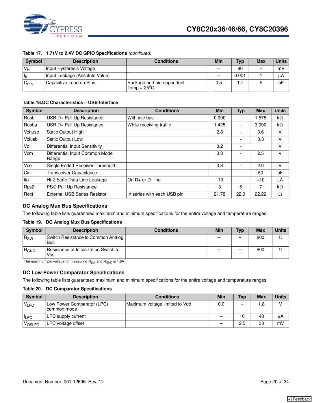
Table 17. 1.71V to 2.4V DC GPIO Specifications (continued)
Symbol | Description | Conditions |
| Min | Typ | Max | Units | |
VH | Input Hysteresis Voltage |
|
| – | 80 | – | mV | |
IIL | Input Leakage (Absolute Value) |
|
| – | 0.001 | 1 |
| μA |
CPIN | Capacitive Load on Pins | Package and pin dependent | 0.5 | 1.7 | 5 |
| pF | |
|
| Temp = 25oC |
|
|
|
|
|
|
Table 18.DC Characteristics – USB Interface |
|
|
|
|
|
|
| |
|
|
|
|
|
|
|
|
|
Symbol | Description | Conditions |
| Min | Typ | Max |
| Units |
Rusbi | USB D+ Pull Up Resistance | With idle bus |
| 0.900 | - | 1.575 |
| kΩ |
|
|
|
|
|
|
|
|
|
Rusba | USB D+ Pull Up Resistance | While receiving traffic |
| 1.425 | - | 3.090 |
| kΩ |
|
|
|
|
|
|
|
|
|
Vohusb | Static Output High |
|
| 2.8 | - | 3.6 |
| V |
|
|
|
|
|
|
|
|
|
Volusb | Static Output Low |
|
|
| - | 0.3 |
| V |
|
|
|
|
|
|
|
|
|
Vdi | Differential Input Sensitivity |
|
| 0.2 | - |
|
| V |
|
|
|
|
|
|
|
|
|
Vcm | Differential Input Common Mode |
|
| 0.8 | - | 2.5 |
| V |
| Range |
|
|
|
|
|
|
|
Vse | Single Ended Receiver Threshold |
|
| 0.8 | - | 2.0 |
| V |
|
|
|
|
|
|
|
|
|
Cin | Transceiver Capacitance |
|
|
| - | 50 |
| pF |
|
|
|
|
|
|
|
|
|
Iio | On D+ or D- line |
| - | +10 |
| μA | ||
|
|
|
|
|
|
|
|
|
Rps2 | PS/2 Pull Up Resistance |
|
| 3 | 5 | 7 |
| kΩ |
|
|
|
|
|
|
|
|
|
Rext | External USB Series Resistor | In series with each USB pin |
| 21.78 | 22.0 | 22.22 |
| Ω |
|
|
|
|
|
|
|
|
|
DC Analog Mux Bus Specifications
The following table lists guaranteed maximum and minimum specifications for the entire voltage and temperature ranges.
Table 19. DC Analog Mux Bus Specifications
Symbol | Description | Conditions | Min | Typ | Max | Units |
RSW | Switch Resistance to Common Analog |
| – | – | 800 | Ω |
| Bus |
|
|
|
|
|
RGND | Resistance of Initialization Switch to |
| – | – | 800 | Ω |
| Vss |
|
|
|
|
|
The maximum pin voltage for measuring RSW and RGND is 1.8V
DC Low Power Comparator Specifications
The following table lists guaranteed maximum and minimum specifications for the entire voltage and temperature ranges.
Table 20. DC Comparator Specifications
Symbol | Description | Conditions | Min | Typ | Max | Units |
VLPC | Low Power Comparator (LPC) | Maximum voltage limited to Vdd | 0.0 | – | 1.8 | V |
| common mode |
|
|
|
|
|
ILPC | LPC supply current |
| – | 10 | 40 | μA |
VOSLPC | LPC voltage offset |
| – | 2.5 | 30 | mV |
Document Number: | Page 20 of 34 |
[+] Feedback