CY8C20x36/46/66, CY8C20396
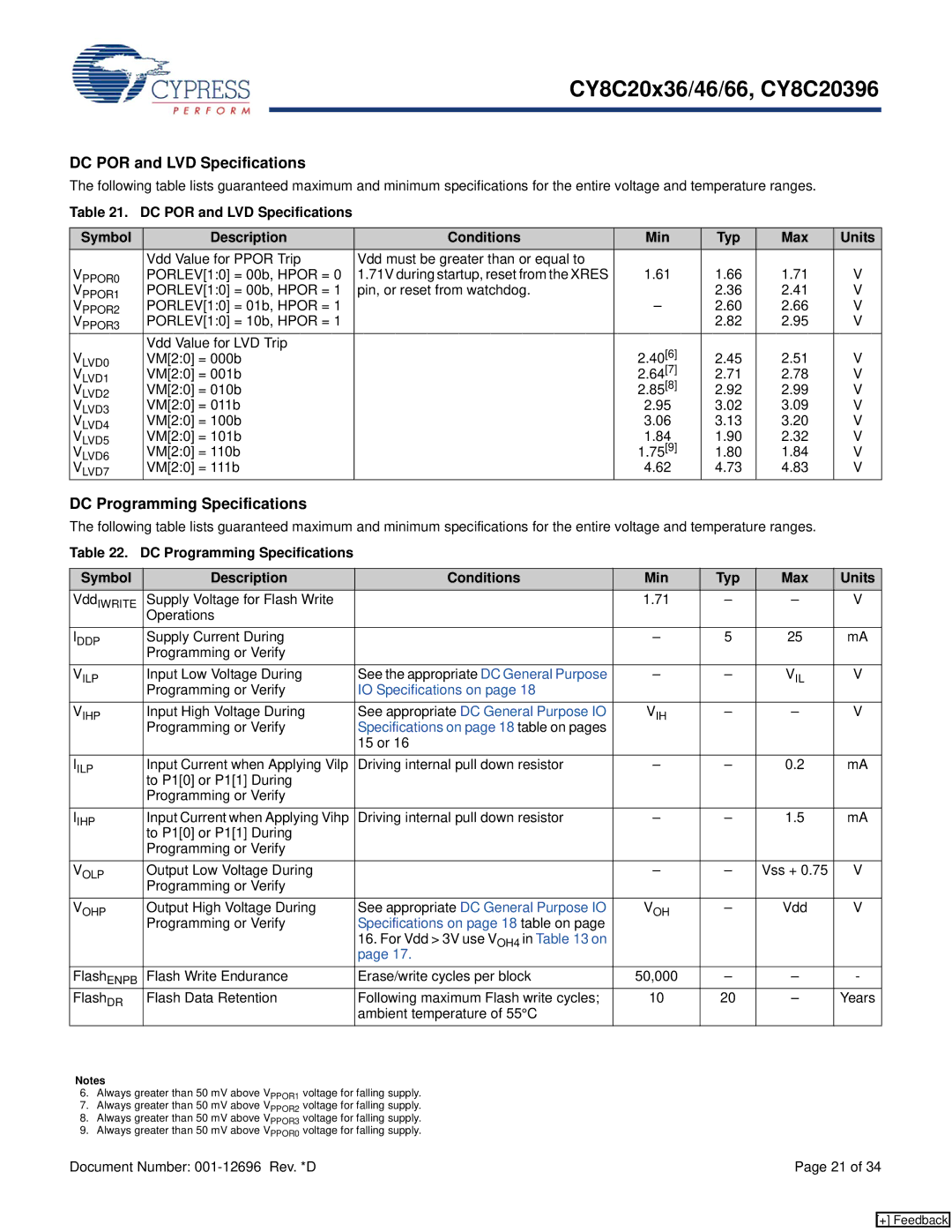
DC POR and LVD Specifications
The following table lists guaranteed maximum and minimum specifications for the entire voltage and temperature ranges.
Table 21. DC POR and LVD Specifications
Symbol | Description | Conditions | Min | Typ | Max | Units |
| Vdd Value for PPOR Trip | Vdd must be greater than or equal to |
|
|
|
|
VPPOR0 | PORLEV[1:0] = 00b, HPOR = 0 | 1.71V during startup, reset from the XRES | 1.61 | 1.66 | 1.71 | V |
VPPOR1 | PORLEV[1:0] = 00b, HPOR = 1 | pin, or reset from watchdog. |
| 2.36 | 2.41 | V |
VPPOR2 | PORLEV[1:0] = 01b, HPOR = 1 |
| – | 2.60 | 2.66 | V |
VPPOR3 | PORLEV[1:0] = 10b, HPOR = 1 |
|
| 2.82 | 2.95 | V |
VLVD0 | Vdd Value for LVD Trip |
| 2.40[6] |
| 2.51 | V |
VM[2:0] = 000b |
| 2.45 | ||||
VLVD1 | VM[2:0] = 001b |
| 2.64[7] | 2.71 | 2.78 | V |
VLVD2 | VM[2:0] = 010b |
| 2.85[8] | 2.92 | 2.99 | V |
VLVD3 | VM[2:0] = 011b |
| 2.95 | 3.02 | 3.09 | V |
VLVD4 | VM[2:0] = 100b |
| 3.06 | 3.13 | 3.20 | V |
VLVD5 | VM[2:0] = 101b |
| 1.84 | 1.90 | 2.32 | V |
VLVD6 | VM[2:0] = 110b |
| 1.75[9] | 1.80 | 1.84 | V |
VLVD7 | VM[2:0] = 111b |
| 4.62 | 4.73 | 4.83 | V |
DC Programming Specifications
The following table lists guaranteed maximum and minimum specifications for the entire voltage and temperature ranges.
Table 22. DC Programming Specifications
Symbol | Description | Conditions | Min | Typ | Max | Units |
VddIWRITE | Supply Voltage for Flash Write |
| 1.71 | – | – | V |
| Operations |
|
|
|
|
|
IDDP | Supply Current During |
| – | 5 | 25 | mA |
| Programming or Verify |
|
|
|
|
|
VILP | Input Low Voltage During | See the appropriate DC General Purpose | – | – | VIL | V |
| Programming or Verify | IO Specifications on page 18 |
|
|
|
|
VIHP | Input High Voltage During | See appropriate DC General Purpose IO | VIH | – | – | V |
| Programming or Verify | Specifications on page 18 table on pages |
|
|
|
|
|
| 15 or 16 |
|
|
|
|
IILP | Input Current when Applying Vilp | Driving internal pull down resistor | – | – | 0.2 | mA |
| to P1[0] or P1[1] During |
|
|
|
|
|
| Programming or Verify |
|
|
|
|
|
IIHP | Input Current when Applying Vihp | Driving internal pull down resistor | – | – | 1.5 | mA |
| to P1[0] or P1[1] During |
|
|
|
|
|
| Programming or Verify |
|
|
|
|
|
VOLP | Output Low Voltage During |
| – | – | Vss + 0.75 | V |
| Programming or Verify |
|
|
|
|
|
VOHP | Output High Voltage During | See appropriate DC General Purpose IO | VOH | – | Vdd | V |
| Programming or Verify | Specifications on page 18 table on page |
|
|
|
|
|
| 16. For Vdd > 3V use VOH4 in Table 13 on |
|
|
|
|
|
| page 17. |
|
|
|
|
FlashENPB | Flash Write Endurance | Erase/write cycles per block | 50,000 | – | – | - |
FlashDR | Flash Data Retention | Following maximum Flash write cycles; | 10 | 20 | – | Years |
|
| ambient temperature of 55°C |
|
|
|
|
Notes
6.Always greater than 50 mV above VPPOR1 voltage for falling supply.
7.Always greater than 50 mV above VPPOR2 voltage for falling supply.
8.Always greater than 50 mV above VPPOR3 voltage for falling supply.
9.Always greater than 50 mV above VPPOR0 voltage for falling supply.
Document Number: | Page 21 of 34 |
[+] Feedback