CYV15G0404RB
Pin Definitions (continued)
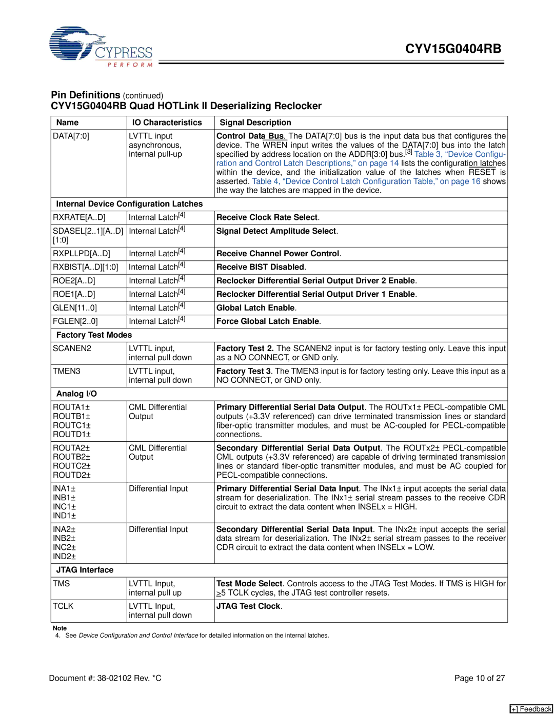
CYV15G0404RB Quad HOTLink II Deserializing Reclocker
Name | IO Characteristics | Signal Description |
|
|
|
DATA[7:0] | LVTTL input | Control Data Bus. The DATA[7:0] bus is the input data bus that configures the |
| asynchronous, | device. The WREN input writes the values of the DATA[7:0] bus into the latch |
| internal | specified by address location on the ADDR[3:0] bus.[3] Table 3, “Device Configu- |
|
| ration and Control Latch Descriptions,” on page 14 lists the configuration latches |
|
| within the device, and the initialization value of the latches when RESET is |
|
| asserted. Table 4, “Device Control Latch Configuration Table,” on page 16 shows |
|
| the way the latches are mapped in the device. |
Internal Device Configuration Latches |
| |
|
|
|
RXRATE[A..D] | Internal Latch[4] | Receive Clock Rate Select. |
SDASEL[2..1][A..D] | Internal Latch[4] | Signal Detect Amplitude Select. |
[1:0] |
|
|
RXPLLPD[A..D] | Internal Latch[4] | Receive Channel Power Control. |
RXBIST[A..D][1:0] | Internal Latch[4] | Receive BIST Disabled. |
ROE2[A..D] | Internal Latch[4] | Reclocker Differential Serial Output Driver 2 Enable. |
ROE1[A..D] | Internal Latch[4] | Reclocker Differential Serial Output Driver 1 Enable. |
GLEN[11..0] | Internal Latch[4] | Global Latch Enable. |
FGLEN[2..0] | Internal Latch[4] | Force Global Latch Enable. |
Factory Test Modes |
| |
|
|
|
SCANEN2 | LVTTL input, | Factory Test 2. The SCANEN2 input is for factory testing only. Leave this input |
| internal pull down | as a NO CONNECT, or GND only. |
TMEN3 | LVTTL input, | Factory Test 3. The TMEN3 input is for factory testing only. Leave this input as a |
| internal pull down | NO CONNECT, or GND only. |
Analog I/O |
|
|
|
|
|
ROUTA1± | CML Differential | Primary Differential Serial Data Output. The ROUTx1± |
ROUTB1± | Output | outputs (+3.3V referenced) can drive terminated transmission lines or standard |
ROUTC1± |
| |
ROUTD1± |
| connections. |
ROUTA2± | CML Differential | Secondary Differential Serial Data Output. The ROUTx2± |
ROUTB2± | Output | CML outputs (+3.3V referenced) are capable of driving terminated transmission |
ROUTC2± |
| lines or standard |
ROUTD2± |
| |
INA1± | Differential Input | Primary Differential Serial Data Input. The INx1± input accepts the serial data |
INB1± |
| stream for deserialization. The INx1± serial stream passes to the receive CDR |
INC1± |
| circuit to extract the data content when INSELx = HIGH. |
IND1± |
|
|
INA2± | Differential Input | Secondary Differential Serial Data Input. The INx2± input accepts the serial |
INB2± |
| data stream for deserialization. The INx2± serial stream passes to the receiver |
INC2± |
| CDR circuit to extract the data content when INSELx = LOW. |
IND2± |
|
|
JTAG Interface |
|
|
|
|
|
TMS | LVTTL Input, | Test Mode Select. Controls access to the JTAG Test Modes. If TMS is HIGH for |
| internal pull up | >5 TCLK cycles, the JTAG test controller resets. |
TCLK | LVTTL Input, | JTAG Test Clock. |
| internal pull down |
|
Note
4. See Device Configuration and Control Interface for detailed information on the internal latches.
Document #: | Page 10 of 27 |
[+] Feedback