CYV15G0404RB
Pin Definitions (continued)
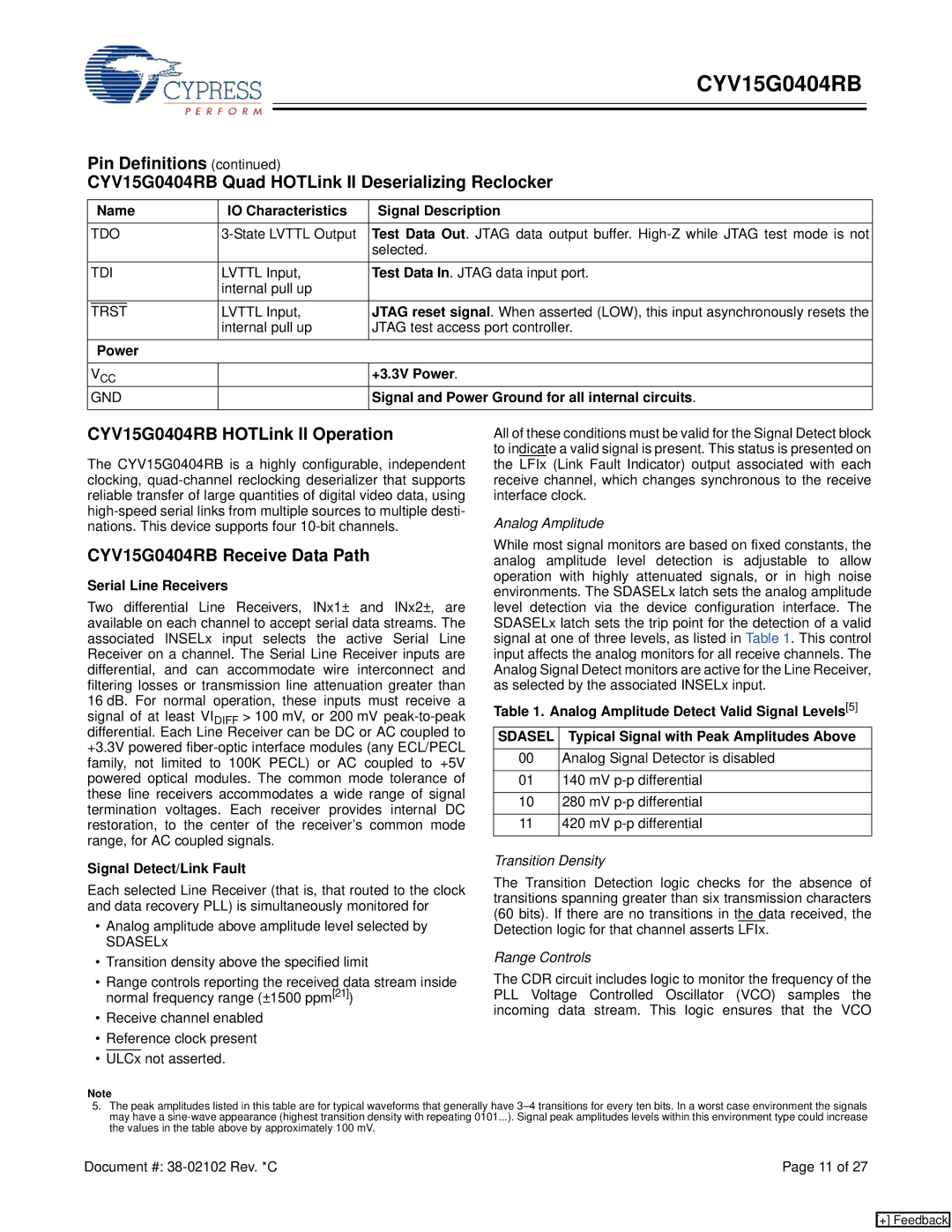
CYV15G0404RB Quad HOTLink II Deserializing Reclocker
| Name | IO Characteristics | Signal Description | |
|
|
|
| |
| TDO | Test Data Out. JTAG data output buffer. | ||
|
|
|
| selected. |
| TDI | LVTTL Input, | Test Data In. JTAG data input port. | |
|
|
| internal pull up |
|
|
|
| LVTTL Input, | JTAG reset signal. When asserted (LOW), this input asynchronously resets the |
| TRST | |||
|
|
| internal pull up | JTAG test access port controller. |
| Power |
|
| |
|
|
|
| |
| VCC |
| +3.3V Power. | |
| GND |
| Signal and Power Ground for all internal circuits. | |
|
|
|
|
|
CYV15G0404RB HOTLink II Operation
The CYV15G0404RB is a highly configurable, independent clocking,
CYV15G0404RB Receive Data Path
Serial Line Receivers
Two differential Line Receivers, INx1± and INx2±, are available on each channel to accept serial data streams. The associated INSELx input selects the active Serial Line Receiver on a channel. The Serial Line Receiver inputs are differential, and can accommodate wire interconnect and filtering losses or transmission line attenuation greater than 16 dB. For normal operation, these inputs must receive a signal of at least VIDIFF > 100 mV, or 200 mV
Signal Detect/Link Fault
Each selected Line Receiver (that is, that routed to the clock and data recovery PLL) is simultaneously monitored for
•Analog amplitude above amplitude level selected by SDASELx
•Transition density above the specified limit
All of these conditions must be valid for the Signal Detect block to indicate a valid signal is present. This status is presented on the LFIx (Link Fault Indicator) output associated with each receive channel, which changes synchronous to the receive interface clock.
Analog Amplitude
While most signal monitors are based on fixed constants, the analog amplitude level detection is adjustable to allow operation with highly attenuated signals, or in high noise environments. The SDASELx latch sets the analog amplitude level detection via the device configuration interface. The SDASELx latch sets the trip point for the detection of a valid signal at one of three levels, as listed in Table 1. This control input affects the analog monitors for all receive channels. The Analog Signal Detect monitors are active for the Line Receiver, as selected by the associated INSELx input.
Table 1. Analog Amplitude Detect Valid Signal Levels[5]
SDASEL Typical Signal with Peak Amplitudes Above
00Analog Signal Detector is disabled
01140 mV
10280 mV
11420 mV
Transition Density
The Transition Detection logic checks for the absence of transitions spanning greater than six transmission characters (60 bits). If there are no transitions in the data received, the Detection logic for that channel asserts LFIx.
Range Controls
•Range controls reporting the received data stream inside normal frequency range (±1500 ppm[21])
•Receive channel enabled
•Reference clock present
•ULCx not asserted.
Note
The CDR circuit includes logic to monitor the frequency of the PLL Voltage Controlled Oscillator (VCO) samples the incoming data stream. This logic ensures that the VCO
5.The peak amplitudes listed in this table are for typical waveforms that generally have
Document #: | Page 11 of 27 |
[+] Feedback