CYV15G0404RB
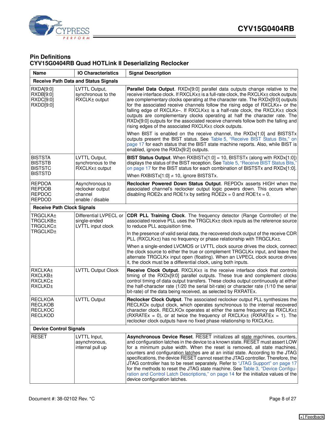
Pin Definitions
CYV15G0404RB Quad HOTLink II Deserializing Reclocker
|
| Name | IO Characteristics | Signal Description | |||
|
|
|
|
|
|
| |
|
| Receive Path Data and Status Signals |
|
|
| ||
|
|
|
|
| |||
|
| RXDA[9:0] | LVTTL Output, | Parallel Data Output. RXDx[9:0] parallel data outputs change relative to the | |||
|
| RXDB[9:0] | synchronous to the | receive interface clock. If RXCLKx± is a | |||
|
| RXDC[9:0] | RXCLK± output | are complementary clocks operating at the character rate. The RXDx[9:0] outputs | |||
|
| RXDD[9:0] |
| for the associated receive channels follow the rising edge of RXCLKx+ or the | |||
|
|
|
|
| falling edge of | ||
|
|
|
|
| outputs are complementary clocks operating at half the character rate. The | ||
|
|
|
|
| RXDx[9:0] outputs for the associated receive channels follow both the falling and | ||
|
|
|
|
| rising edges of the associated RXCLKx± clock outputs. | ||
|
|
|
|
| When BIST is enabled on the receive channel, the RXDx[1:0] and BISTSTx | ||
|
|
|
|
| outputs present the BIST status. See Table 5, “Receive BIST Status Bits,” on | ||
|
|
|
|
| page 17 for each status that the BIST state machine reports. Also, while BIST is | ||
|
|
|
|
| enabled, ignore the RXDx[9:2] outputs. | ||
|
| BISTSTA | LVTTL Output, | BIST Status Output. When RXBISTx[1:0] = 10, BISTSTx (along with RXDx[1:0]) | |||
|
| BISTSTB | synchronous to the | displays the status of the BIST reception. See Table 5, “Receive BIST Status Bits,” | |||
|
| BISTSTC | RXCLKx± output | on page 17 for the BIST status for each combination of BISTSTx and RXDx[1:0]. | |||
|
| BISTSTD |
| When RXBISTx[1:0] ≠ 10, ignore BISTSTx. | |||
|
|
|
|
| |||
|
|
|
|
| |||
|
| REPDOA | Asynchronous to | Reclocker Powered Down Status Output. REPDOx asserts HIGH when the | |||
|
| REPDOB | reclocker output | associated channel’s reclocker output logic powers down. This occurs when | |||
|
| REPDOC | channel | disabling ROE2x and ROE1x by setting ROE2x = 0 and ROE1x = 0. | |||
|
| REPDOD | enable / disable |
|
|
| |
|
| Receive Path Clock Signals |
|
|
| ||
|
|
|
|
| |||
|
| TRGCLKA± | Differential LVPECL or | CDR PLL Training Clock. The frequency detector (Range Controller) of the | |||
|
| TRGCLKB± | associated receive PLL uses the TRGCLKx± clock inputs as the reference source | ||||
|
| TRGCLKC± | LVTTL input clock | to reduce PLL acquisition time. | |||
|
| TRGCLKD± |
| In the presence of valid serial data, the recovered clock output of the receive CDR | |||
|
|
|
|
| PLL (RXCLKx±) has no frequency or phase relationship with TRGCLKx±. | ||
|
|
|
|
| When a | ||
|
|
|
|
| the clock source to either the true or complement TRGCLKx input, and leave the | ||
|
|
|
|
| alternate TRGCLKx input open (floating). When an LVPECL clock source drives | ||
|
|
|
|
| it, the clock must be a differential clock, using both inputs. | ||
|
| RXCLKA± | LVTTL Output Clock | Receive Clock Output. RXCLKx± is the receive interface clock that controls | |||
|
| RXCLKB± |
| timing of the RXDx[9:0] parallel outputs. These true and complement clocks | |||
|
| RXCLKC± |
| control timing of data output transfers. These clocks output continuously at either | |||
|
| RXCLKD± |
| the | |||
|
|
|
|
| |||
|
| RECLKOA | LVTTL Output | Reclocker Clock Output. The associated reclocker output PLL synthesizes the | |||
|
| RECLKOB |
| RECLKOx output clock, which operates synchronous to the internal recovered | |||
|
| RECLKOC |
| character clock. RECLKOx operates at either the same frequency as RXCLKx± | |||
|
| RECLKOD |
| (RXRATEx = 0), or at twice the frequency of RXCLKx± (RXRATEx = 1). The | |||
|
|
|
|
| reclocker clock outputs have no fixed phase relationship to RXCLKx±. | ||
|
| Device Control Signals |
|
|
| ||
|
|
|
|
|
|
|
|
|
|
|
| LVTTL Input, | Asynchronous Device Reset. |
| initializes all state machines, counters, |
|
| RESET | RESET | ||||
|
|
|
| asynchronous, | and configuration latches in the device to a known state. RESET must assert LOW | ||
|
|
|
| internal pull up | for a minimum pulse width. When the reset is removed, all state machines, | ||
|
|
|
|
| counters and configuration latches are at an initial state. According to the JTAG | ||
|
|
|
|
| specifications, the device RESET cannot reset the JTAG controller. Therefore, the | ||
|
|
|
|
| JTAG controller has to be reset separately. Refer to “JTAG Support” on page 17 | ||
|
|
|
|
| for the methods to reset the JTAG state machine. See Table 3, “Device Configu- | ||
|
|
|
|
| ration and Control Latch Descriptions,” on page 14 for the initialize values of the | ||
|
|
|
|
| device configuration latches. | ||
Document #: |
|
| Page 8 of 27 | ||||
[+] Feedback