Configuration and Operation
CS0
ECB
A2...A24
BCLK
OE
LBA
DQM3_EB3
FLASH_RST D0.15
DQM1_EB1
D16..31
VCC VCC VCC
CS
WP
ACC
8MX16-Bit Burst Flash
RDY
A0...A22
CLK
OE
AVD
WE
RESET
D0..15
WE
D0.15
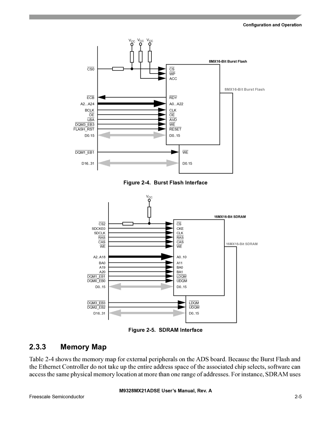
Figure 2-4. Burst Flash Interface
CS2
SDCKE0 SDCLK RAS CAS WE
A2..A18
BA0
A19
A20 DQM1_EB1 DQM0_EB0
D0..15
DQM3_EB3 DQM2_EB2
D16..31
VCC |
| |
| ||
CS |
| |
CKE |
| |
CLK |
| |
RAS |
| |
CAS | ||
WE | ||
| ||
A0..10 |
| |
A11 |
| |
BA0 |
| |
BA1 |
| |
LDQM |
| |
UDQM |
| |
D0..15 |
| |
| LDQM | |
| UDQM | |
| D0..15 |
Figure 2-5. SDRAM Interface
2.3.3Memory Map
Table
| M9328MX21ADSE User’s Manual, Rev. A |
Freescale Semiconductor |