Support Information
3.7USB OTG Connector
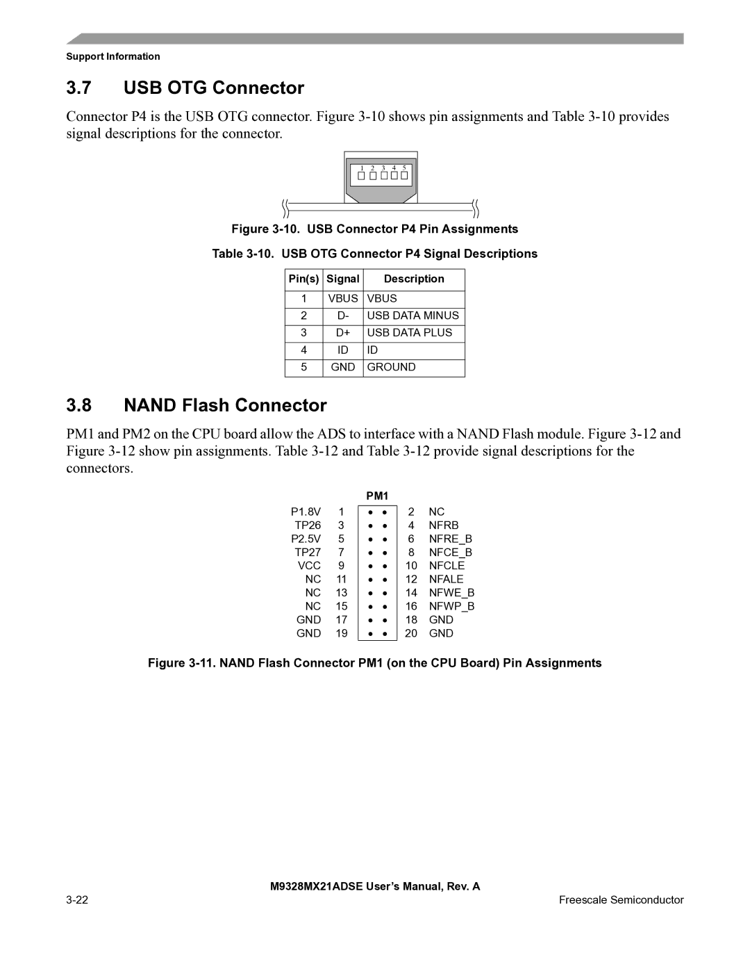
Connector P4 is the USB OTG connector. Figure
1 | 2 | 3 | 4 | 5 |
Figure 3-10. USB Connector P4 Pin Assignments
Table 3-10. USB OTG Connector P4 Signal Descriptions
Pin(s) | Signal | Description |
|
|
|
1 | VBUS | VBUS |
|
|
|
2 | D- | USB DATA MINUS |
|
|
|
3 | D+ | USB DATA PLUS |
|
|
|
4 | ID | ID |
|
|
|
5 | GND | GROUND |
|
|
|
3.8NAND Flash Connector
PM1 and PM2 on the CPU board allow the ADS to interface with a NAND Flash module. Figure
PM1
P1.8V 1 • •
TP26 3 • •
P2.5V 5 • •
TP27 7 • •
VCC 9 • • NC 11 • • NC 13 • • NC 15 • • GND 17 • • GND 19 • •
2 | NC |
4 | NFRB |
6NFRE_B
8NFCE_B
10 NFCLE
12 NFALE
14 NFWE_B
16 NFWP_B
18 GND
20 GND
Figure 3-11. NAND Flash Connector PM1 (on the CPU Board) Pin Assignments
| M9328MX21ADSE User’s Manual, Rev. A |
Freescale Semiconductor |