General Information
+5V IN |
|
|
|
|
|
|
| OFF |
|
|
|
|
| P3 |
|
|
|
|
|
|
|
|
|
|
|
|
|
|
|
|
|
|
|
|
|
|
|
|
|
| |||
|
|
|
|
|
|
|
|
|
|
|
|
|
|
|
|
|
|
| |||
|
|
|
|
|
|
|
|
|
|
|
|
|
|
|
|
|
|
| |||
P8 |
|
|
|
|
|
|
| ON |
|
|
|
|
| EXT UART DCE |
|
|
| ||||
|
|
|
|
|
|
|
|
|
|
|
|
|
|
|
|
| |||||
|
|
|
|
|
|
|
|
| SW1 |
|
|
|
|
|
|
|
|
| |||
|
|
|
|
|
|
|
|
| P9 |
|
|
| |||||||||
|
|
|
|
|
|
|
|
|
|
|
|
|
|
|
| ||||||
|
|
|
|
|
|
|
|
|
|
|
|
| ETHERNET |
|
|
| |||||
| F1 |
|
|
|
|
|
|
|
|
|
|
|
|
|
|
|
|
| |||
| 2A |
|
|
|
|
|
|
|
|
|
|
|
|
|
|
|
|
| |||
BASE BOARD
P2 |
|
|
|
|
|
|
|
| P1 |
|
|
|
|
|
|
|
|
|
|
| P4 |
|
|
|
|
|
|
|
|
| P7 | |
|
|
|
|
|
|
|
|
|
|
|
|
|
|
|
|
|
|
|
|
|
|
|
|
|
|
|
| |||||
|
|
|
|
|
|
|
|
|
|
|
|
|
|
|
|
|
|
|
|
|
|
|
|
|
|
|
| |||||
|
|
|
|
|
|
|
|
|
|
|
|
|
|
|
|
|
|
|
|
|
|
|
|
|
|
|
| |||||
|
|
|
|
|
|
|
|
|
|
|
|
|
|
|
|
|
|
|
|
|
| U16 IrDA |
| |||||||||
| UART4 DTE |
|
| UART1 DCE |
|
|
|
| USB OTG |
|
| |||||||||||||||||||||
|
|
| DTR | NC | DSR | NC | CD |
| NC | RI |
|
|
|
|
|
|
|
|
|
|
|
|
|
|
| |||||||
ACT |
|
|
|
|
|
|
|
|
|
|
|
| 3 |
|
|
|
| VR1 |
|
|
|
|
|
|
|
| ||||||
|
|
|
|
|
|
|
|
|
|
|
|
|
|
|
|
|
|
|
|
|
|
|
| |||||||||
SD2_D0 |
|
| SD2_D1 |
|
|
| SD2_D2 |
|
|
|
| SD2_D3 |
|
| 2 |
|
|
|
|
|
|
|
|
|
|
|
| CON | ||||
|
|
|
|
|
|
|
|
|
|
| 1 |
|
|
|
|
|
|
|
|
|
|
|
| |||||||||
|
|
|
|
|
|
|
|
|
|
|
|
|
|
|
| BATT EM | ||||||||||||||||
|
|
| J3 |
| J4 |
| J5 |
|
| J6 |
|
|
|
|
|
| ||||||||||||||||
|
|
|
|
|
|
|
|
|
|
|
|
| LCD | |||||||||||||||||||
|
|
|
|
|
|
|
|
|
|
|
|
|
|
|
|
|
|
|
| |||||||||||||
|
|
|
|
|
|
|
|
|
|
|
|
|
|
|
|
|
|
|
|
|
|
|
|
|
|
|
|
|
|
| ||
| CPU BOARD |
|
|
|
|
|
|
|
|
|
|
|
|
|
|
|
|
|
|
|
|
|
| |||||||||
|
|
|
|
|
|
|
|
|
|
|
|
|
|
|
|
|
|
|
|
|
|
|
|
| ||||||||
|
|
|
|
|
|
|
|
|
|
|
|
|
| PX1/PY1 |
|
|
|
|
|
|
|
|
|
|
|
|
|
|
| |||
SW2
RESET
|
|
| 5V PWR |
| LED1 | |||
|
|
| VCC PWR |
| LED2 | |||
|
|
|
| |||||
|
|
| STAT2 |
| LED3 | |||
|
|
|
| |||||
|
|
| STAT1 |
| LED4 | |||
|
|
|
| |||||
|
|
| BUS ACT |
| LED7 | |||
|
|
|
| |||||
|
|
|
| BUZZER |
| |||
|
|
|
|
|
|
|
|
|
|
|
|
|
| P10 |
| ||
|
|
|
|
|
| |||
|
|
|
|
| LINE IN | |||
|
|
|
|
| P11 |
| ||
|
|
|
|
|
| |||
|
|
|
|
|
| |||
|
|
|
|
| MIC IN | |||
|
|
|
|
|
|
|
|
|
LED6 LED5
LINK ACT
S2
1 ![]()
![]()
![]() BOOT0
BOOT0
2 ![]() BOOT1
BOOT1
3 ![]()
![]()
![]() BOOT2
BOOT2
4 ![]() BOOT3
BOOT3
5 ![]()
![]()
![]() CLKMODE0
CLKMODE0
6 ![]()
![]()
![]() CLKMODE1
CLKMODE1
7![]()
![]()
![]() SW1 IRQ
SW1 IRQ
8![]()
![]()
![]() SW2 READ
SW2 READ
S1
1![]() UART1_ON
UART1_ON
2![]() UART4_ON
UART4_ON
3![]() IrDA_ON
IrDA_ON
4![]() NEXUS_EN
NEXUS_EN
5![]()
![]()
![]() JTAG_CTRL
JTAG_CTRL
6![]()
![]()
![]() TONE_OUT
TONE_OUT
7![]() PEN_CS_B
PEN_CS_B
8![]() PEN_IRQ_B
PEN_IRQ_B
P20 |
|
|
|
|
|
|
|
|
|
|
|
|
|
|
| TV ENCODER |
| P13 | |||||||
|
|
|
|
|
|
|
|
|
|
|
|
|
|
|
| ||||||||||
|
|
|
|
|
|
|
|
|
|
|
|
|
|
|
| ||||||||||
|
|
|
|
| PK1 |
|
|
|
|
| CON | ||||||||||||||
|
|
|
|
|
|
|
|
|
|
| |||||||||||||||
|
|
|
|
|
|
|
|
|
|
|
|
|
|
|
|
|
|
| |||||||
|
|
|
|
|
|
|
|
|
|
|
|
|
|
|
|
|
|
|
|
|
|
|
| ||
|
|
|
|
|
|
|
|
|
|
|
|
|
|
|
|
|
|
|
|
|
| ||||
|
|
|
|
|
|
|
|
|
|
|
|
|
|
|
|
|
|
|
|
|
| ||||
|
|
|
|
|
|
|
|
|
|
|
|
|
|
| U6 |
|
|
| |||||||
|
|
|
|
|
|
|
|
|
|
|
|
|
|
|
|
|
|
| |||||||
|
|
|
|
|
|
|
|
|
|
|
|
|
|
|
| U7 |
|
| |||||||
|
|
|
|
|
| U5 |
|
|
|
|
|
|
|
|
|
|
|
|
|
|
|
|
|
| |
| CARD |
|
|
|
|
|
|
|
|
|
|
|
|
|
|
|
|
|
|
|
|
|
| ||
| PM1 |
|
|
|
| CPU |
|
|
|
| U8 |
| U9 |
| P5 | ||||||||||
|
|
|
|
|
|
|
|
|
|
|
|
|
|
|
|
|
|
|
|
| |||||
|
|
|
|
|
|
|
|
|
|
|
|
|
|
|
|
|
|
|
|
|
|
| |||
|
|
|
|
|
|
|
|
|
|
|
|
|
|
|
|
|
|
|
|
|
|
|
|
|
|
|
|
|
|
|
|
|
|
|
|
|
|
|
|
|
|
|
|
|
|
|
|
|
|
|
|
|
|
|
|
|
|
|
|
|
|
|
|
|
|
|
|
|
|
|
|
|
|
|
|
| |
|
| PM2 |
|
| J3 | J2 |
|
|
|
|
|
|
|
|
|
|
| ||||||||
|
|
|
|
|
| J1 |
|
|
|
|
|
|
|
|
|
|
| ||||||||
|
|
|
|
|
|
|
|
|
|
|
|
|
|
| PK2 |
|
|
|
|
|
|
|
| ||
| FLASHNAND |
|
|
|
|
|
|
|
|
|
|
|
|
|
|
|
|
|
| CONKEYPAD |
| ||||
|
|
|
|
|
|
|
|
|
|
|
|
|
|
|
|
|
|
|
|
|
|
| |||
|
|
|
|
|
|
|
|
|
|
|
| PX2/PY2 |
|
|
|
|
|
|
|
| |||||
|
|
|
|
|
|
|
|
|
|
|
|
|
|
|
|
|
|
|
| ||||||
P6
|
|
|
| P12 |
|
| J7 |
|
| ||||
|
|
|
| HEADPHONE |
|
| ONE WIRE |
|
| ||||
|
|
|
| PE3 |
|
|
| ||||||
|
|
|
|
|
|
|
|
|
|
| |||
|
|
|
|
|
|
|
|
|
|
| |||
|
|
|
|
|
|
|
|
|
|
|
|
|
|
|
|
|
|
|
|
|
|
|
|
|
|
|
|
|
|
|
|
|
|
|
| EXP CON 2 |
|
| |||
|
|
|
|
|
|
|
|
|
|
|
|
|
|
|
| PE2 |
|
|
|
|
|
|
|
|
| PE1 |
|
|
|
| SD/MMC |
|
|
|
|
|
|
|
|
|
|
|
|
|
|
|
|
|
|
|
|
|
|
| |||||||
|
| EXP CON 1 |
|
|
|
|
|
|
| CSI |
|
|
|
|
|
|
|
|
| ||||
|
|
|
|
|
|
|
|
|
|
|
|
|
|
|
|
|
|
|
|
|
|
|
|
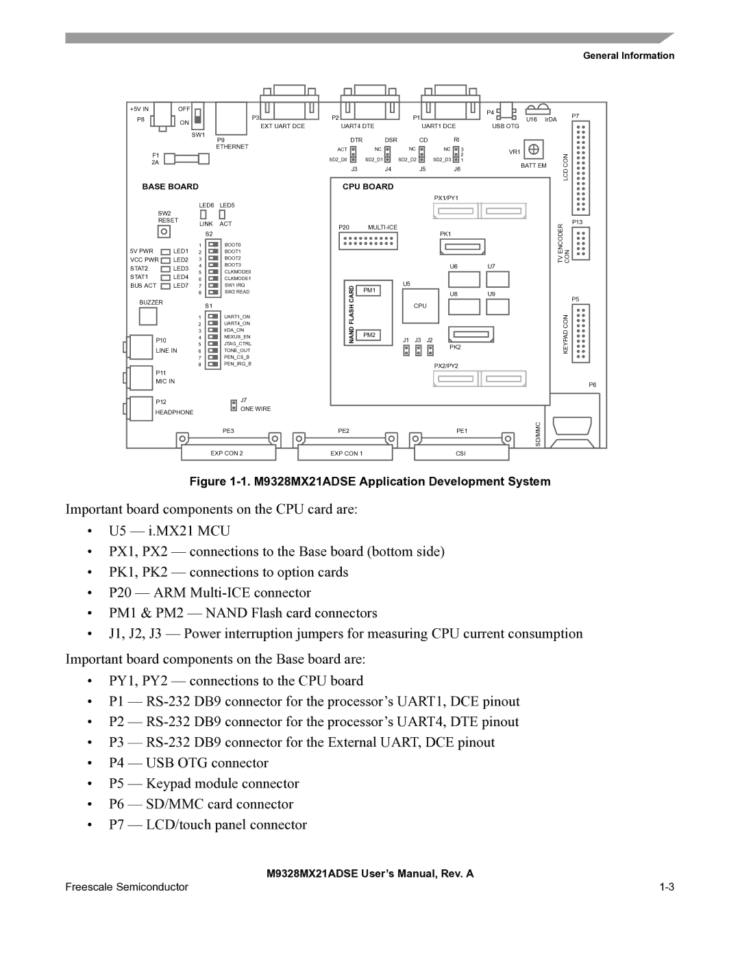
Figure 1-1. M9328MX21ADSE Application Development System
Important board components on the CPU card are:
•U5 — i.MX21 MCU
•PX1, PX2 — connections to the Base board (bottom side)
•PK1, PK2 — connections to option cards
•P20 — ARM
•PM1 & PM2 — NAND Flash card connectors
•J1, J2, J3 — Power interruption jumpers for measuring CPU current consumption
Important board components on the Base board are:
•PY1, PY2 — connections to the CPU board
•P1 —
•P2 —
•P3 —
•P4 — USB OTG connector
•P5 — Keypad module connector
•P6 — SD/MMC card connector
•P7 — LCD/touch panel connector
| M9328MX21ADSE User’s Manual, Rev. A |
Freescale Semiconductor |