Support Information
Table 3-4. CPU to Option Card PK2 Connector Signals (continued)
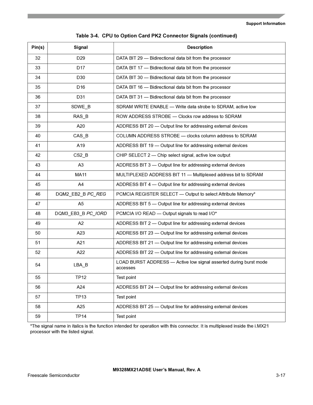
Pin(s) | Signal | Description | |
|
|
| |
32 | D29 | DATA BIT 29 — Bidirectional data bit from the processor | |
|
|
| |
33 | D17 | DATA BIT 17 — Bidirectional data bit from the processor | |
|
|
| |
34 | D30 | DATA BIT 30 — Bidirectional data bit from the processor | |
|
|
| |
35 | D16 | DATA BIT 16 — Bidirectional data bit from the processor | |
|
|
| |
36 | D31 | DATA BIT 31 — Bidirectional data bit from the processor | |
|
|
| |
37 | SDWE_B | SDRAM WRITE ENABLE — Write data strobe to SDRAM, active low | |
|
|
| |
38 | RAS_B | ROW ADDRESS STROBE — Clocks row address to SDRAM | |
|
|
| |
39 | A20 | ADDRESS BIT 20 — Output line for addressing external devices | |
|
|
| |
40 | CAS_B | COLUMN ADDRESS STROBE — clocks column address to SDRAM | |
|
|
| |
41 | A19 | ADDRESS BIT 19 — Output line for addressing external devices | |
|
|
| |
42 | CS2_B | CHIP SELECT 2 — Chip select signal, active low output | |
|
|
| |
43 | A3 | ADDRESS BIT 3 — Output line for addressing external devices | |
|
|
| |
44 | MA11 | MULTIPLEXED ADDRESS BIT 11 — Multiplexed address bit to SDRAM | |
|
|
| |
45 | A4 | ADDRESS BIT 4 — Output line for addressing external devices | |
|
|
| |
46 | DQM2_EB2_B PC_REG | PCMCIA REGISTER SELECT — Output to select Attribute Memory* | |
|
|
| |
47 | A5 | ADDRESS BIT 5 — Output line for addressing external devices | |
|
|
| |
48 | DQM3_EB3_B PC_IORD | PCMCIA I/O READ — Output signals to read I/O* | |
|
|
| |
49 | A2 | ADDRESS BIT 2 — Output line for addressing external devices | |
|
|
| |
50 | A23 | ADDRESS BIT 23 — Output line for addressing external devices | |
|
|
| |
51 | A21 | ADDRESS BIT 21 — Output line for addressing external devices | |
|
|
| |
52 | A22 | ADDRESS BIT 22 — Output line for addressing external devices | |
|
|
| |
54 | LBA_B | LOAD BURST ADDRESS — Active low signal asserted during burst mode | |
accesses | |||
|
| ||
|
|
| |
55 | TP12 | Test point | |
|
|
| |
56 | A24 | ADDRESS BIT 24 — Output line for addressing external devices | |
|
|
| |
57 | TP13 | Test point | |
|
|
| |
58 | A25 | ADDRESS BIT 25 — Output line for addressing external devices | |
|
|
| |
59 | TP14 | Test point | |
|
|
|
*The signal name in italics is the function intended for operation with this connector. It is multiplexed inside the i.MX21 processor with the listed signal.
| M9328MX21ADSE User’s Manual, Rev. A |
Freescale Semiconductor |