Configuration and Operation
2.3.10.2Output I/O
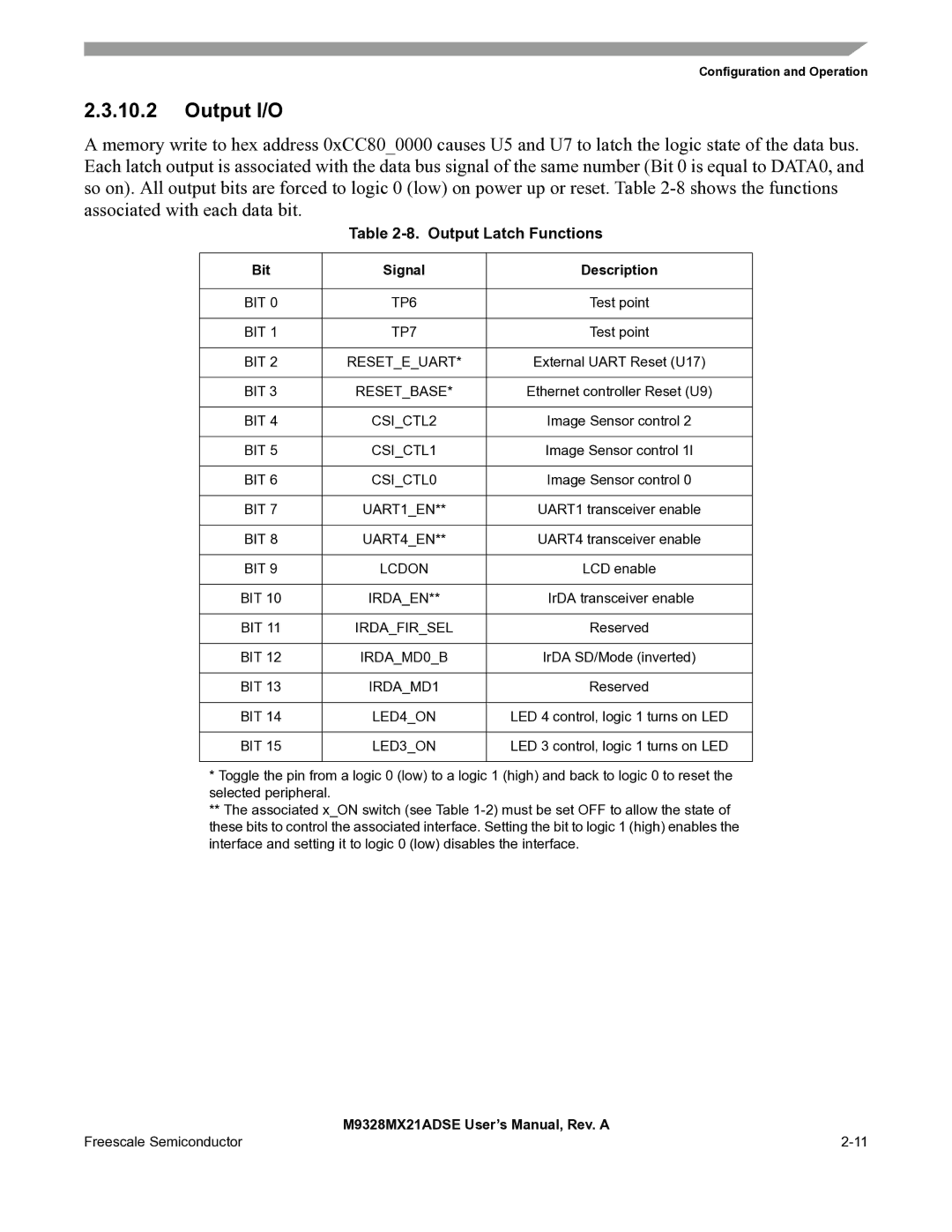
A memory write to hex address 0xCC80_0000 causes U5 and U7 to latch the logic state of the data bus. Each latch output is associated with the data bus signal of the same number (Bit 0 is equal to DATA0, and so on). All output bits are forced to logic 0 (low) on power up or reset. Table
Table 2-8. Output Latch Functions
Bit | Signal | Description |
|
|
|
BIT 0 | TP6 | Test point |
|
|
|
BIT 1 | TP7 | Test point |
|
|
|
BIT 2 | RESET_E_UART* | External UART Reset (U17) |
|
|
|
BIT 3 | RESET_BASE* | Ethernet controller Reset (U9) |
|
|
|
BIT 4 | CSI_CTL2 | Image Sensor control 2 |
|
|
|
BIT 5 | CSI_CTL1 | Image Sensor control 1l |
|
|
|
BIT 6 | CSI_CTL0 | Image Sensor control 0 |
|
|
|
BIT 7 | UART1_EN** | UART1 transceiver enable |
|
|
|
BIT 8 | UART4_EN** | UART4 transceiver enable |
|
|
|
BIT 9 | LCDON | LCD enable |
|
|
|
BIT 10 | IRDA_EN** | IrDA transceiver enable |
|
|
|
BIT 11 | IRDA_FIR_SEL | Reserved |
|
|
|
BIT 12 | IRDA_MD0_B | IrDA SD/Mode (inverted) |
|
|
|
BIT 13 | IRDA_MD1 | Reserved |
|
|
|
BIT 14 | LED4_ON | LED 4 control, logic 1 turns on LED |
|
|
|
BIT 15 | LED3_ON | LED 3 control, logic 1 turns on LED |
|
|
|
*Toggle the pin from a logic 0 (low) to a logic 1 (high) and back to logic 0 to reset the selected peripheral.
**The associated x_ON switch (see Table
| M9328MX21ADSE User’s Manual, Rev. A |
Freescale Semiconductor |