Alternative, the device must issue the SMART
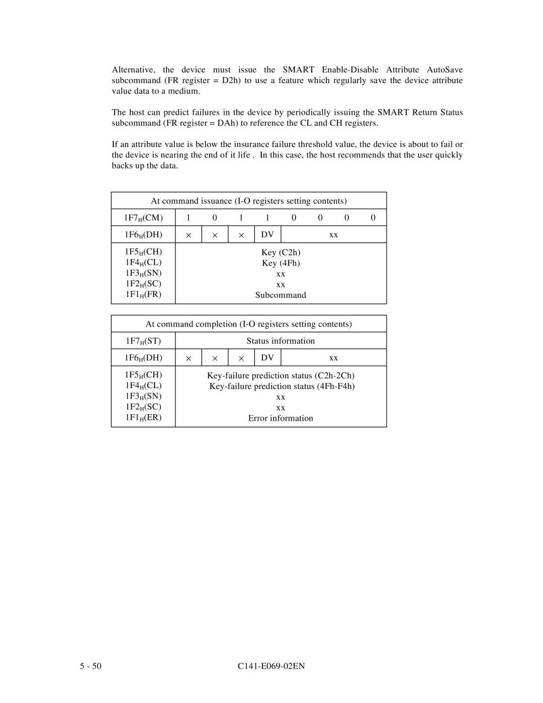
The host can predict failures in the device by periodically issuing the SMART Return Status subcommand (FR register = DAh) to reference the CL and CH registers.
If an attribute value is below the insurance failure threshold value, the device is about to fail or the device is nearing the end of it life . In this case, the host recommends that the user quickly backs up the data.
At command issuance
1F7H(CM) | 1 | 0 | 1 | 1 | 0 | 0 | 0 | 0 | |
|
|
|
|
|
|
|
|
|
|
1F6H(DH) | × | × | × | DV |
|
|
| xx |
|
|
|
|
|
|
|
|
|
| |
1F5H(CH) |
|
|
| Key (C2h) |
|
|
| ||
1F4H(CL) |
|
|
| Key (4Fh) |
|
|
| ||
1F3H(SN) |
|
|
|
| xx |
|
|
| |
1F2H(SC) |
|
|
|
| xx |
|
|
| |
1F1H(FR) |
|
|
| Subcommand |
|
|
| ||
|
|
|
|
|
|
|
|
|
|
At command completion
1F7H(ST) |
|
|
| Status information |
| ||
|
|
|
|
|
|
|
|
1F6H(DH) | × | × | × |
| DV |
| xx |
|
|
|
|
|
| ||
1F5H(CH) |
| ||||||
1F4H(CL) |
| ||||||
1F3H(SN) |
|
|
|
| xx |
| |
1F2H(SC) |
|
|
|
| xx |
| |
1F1H(ER) |
|
|
| Error information |
| ||
|
|
|
|
|
|
|
|
5 - 50 |
|