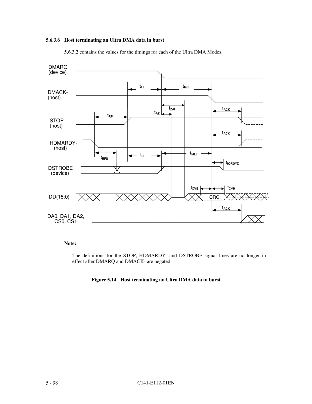
C141-E112-01EN
MPG3xxxAH DISK DRIVES PRODUCT MANUAL
59,6,215&25
C141-E112-01EN
7KHFRQWHQWVRIWKLVPDQXDOLVVXEMHFWWRFKDQJH ZLWKRXWSULRUQRWLFH
This page is intentionally left blank
DEVICE OVERVIEW DEVICE CONFIGURATION INSTALLATION CONDITIONS
This manual MPG3xxxAH DISK DRIVES MAINTENANCE MANUAL C141-F047
MAINTENANCE AND DIAGNOSIS REMOVAL AND REPLACEMENT PROCEDURE
MANUAL ORGANIZATION MPG3xxxAH DISK DRIVES PRODUCT MANUAL C141-E112
This page is intentionally left blank
DEVICE CONFIGURATION
PREFACE
INSTALLATION CONDITIONS
Chapter
Conventions for Alert Messages
C141-E112-01EN
LIABILITY EXCEPTION
This page is intentionally left blank
CHAPTER
CONTENTS
CHAPTER
CHAPTER
CHAPTER
Signal assignment on the connector
Interface signals
Command block registers
Host Commands
CHAPTER
TABLES
WRITE SECTORS command protocol
Protocol for command abort
Protocol for the command execution without data transfer
Multiword DMA data transfer timing mode
TABLES
This page is intentionally left blank
1.1 Features 1.2 Device Specifications 1.3 Power Requirements
CHAPTER 1 DEVICE OVERVIEW
1.4 Environmental Specifications 1.5 Acoustic Noise
1.6 Shock and Vibration 1.7 Reliability 1.8 Error Rate
1.1.3 Interface
1.1.2 Adaptability
5 Error correction and retry by ECC
6 Write cache
C141-E112-01EN
Specifications
1.2 Device Specifications 1.2.1 Specifications summary
16.7 MB/s Max. burst PIO mode 4, burst DMA mode
66.6 MB/s Max. burst ultra DMA mode
1.2.2 Model and product number
1.3 Power Requirements
Table 1.2 Model names and product numbers
Model
C141-E112-01EN
Table 1.3 Current and power dissipation
Figure 1.1 Current fluctuation Typ. when power is turned on
Environmental specifications
1.4 Environmental Specifications
Table 1.5 Acoustic noise specification
1.5 Acoustic Noise
Table 1.6 Shock and vibration specification
1.6 Shock and Vibration
1.7 Reliability
1.9 Media Defects
1.8 Error Rate
2.1 Device Configuration 2.2 System Configuration
CHAPTER 2 DEVICE CONFIGURATION
2.1 Device Configuration
Figure 2.1 Disk drive outerview
MPG3102AH 1 disks MPG3153AH 2 disks MPG3204AH 2 disks 2 Head
1 Disk
3 Spindle motor
The disks are rotated by a direct drive Hall-less DC motor 4 Actuator
Figure 2.2 1 drive system configuration 2.2.3 2 drives connection
2.2 System Configuration 2.2.1 ATA interface
Figure 2.3 2 drives configuration
2.2.2 1 drive connection
HA host adapter consists of address decoder, driver, and receiver. ATA is an abbreviation of AT attachment. The disk drive is conformed to the ATA-5 interface
CHAPTER 3 INSTALLATION CONDITIONS
3.1 Dimensions 3.2 Handling Cautions 3.3 Mounting
3.4 Cable Connections 3.5 Jumper Settings 3.1 Dimensions
C141-E112-01EN
Figure 3.1 Dimensions
3.2 Handling Cautions
3.2.2 Installation
3.2.1 General notes
Figure 3.2 Handling cautions
Figure 3.3 Direction
3.3 Mounting
Figure 3.5 Mounting frame structure
Figure 3.4 Limitation of side-mounting
Table 3.1 Surface temperature measurement points and standard values
Figure 3.6 Surface temperature measurement points
Figure 3.7 Service area
∙ Power supply connector CN1 ∙ ATA interface connector CN1
3.4 Cable Connections 3.4.1 Device connector
Power supply connector CN1 Mode Setting Pins ATA interface connector
Figure 3.8 Connector locations
Table 3.2 Cable connector specifications
3.4.2 Cable connector specifications
3.4.3 Device connection
Figure 3.9 Cable connections
3.4.4 Power supply connector CN1
Figure 3.10 Power supply connector pins CN1
3.4.5 System configuration for Ultra DMA
Cable configuration
Figure 3.12 Cable type detection using CBLID- signal Host sensing the condition of the CBLID- signal
DC Power Connector
3.5 Jumper Settings 3.5.1 Location of setting jumpers
Interface Connector
Figure 3.14 Jumper location
Figure 3.15 Factory default setting 3.5.3 Jumper configuration
3.5.2 Factory default setting
Figure 3.16 Jumper setting of master or slave device
DC Power
Figure 3.17 Jumper setting of Cable Select
Figure 3.18 Example 1 of Cable Select
Figure 3.19 Example 2 of Cable Select
Master Device
3 Special jumper settings a 2.1 GB clip Limit capacity to 2.1 GB
Slave Device
Cable Select
4.1 Outline 4.2 Subassemblies 4.3 Circuit Configuration
CHAPTER 4 THEORY OF DEVICE OPERATION
4.4 Power-on sequence 4.5 Self-calibration 4.6 Read/write Circuit
4.7 Servo Control
Figure 4.1 Head structure
4.2.2 Head
S p i n d l eA c t u a t o r
4.2.3 Spindle
4.2.4 Actuator
4.2.5 Air filter
4.3 Circuit Configuration
Page
4.4 Power-on Sequence
Figure 4.3 Power-on operation sequence
4.5 Self-calibration
4.5.1 Self-calibration contents
4.5.3 Command processing during self-calibration
4.6 Read/write Circuit
4.6.1 Read/write preamplifier PreAMP
4.6.2 Write circuit
4.6.3 Read circuit
4.6.4 Synthesizer circuit
Table 4.1 Transfer rate of each zone
4.7 Servo Control
Figure 4.4 Block diagram of servo control circuit
4.7.1 Servo control circuit
Servo burst capture
Servoframe 96 servoframes per revolution
Figure 4.5 Physical sector servo configuration on disk surface
2 Servo burst capture circuit
5 Power amplifier
3 A/D converter ADC
4 D/A converter DAC
4.7.3 Servo frame format
4.7.2 Data-surface servo format
Figure 4.6 96 servo frames in each track
4.7.4 Actuator motor control
4.7.5 Spindle motor control
2 Acceleration mode
3 Stable rotation mode
C141-E112-01EN
INTERFACE
CHAPTER
5.1 Physical Interface 5.2 Logical Interface 5.3 Host Commands
5.4 Command Protocol 5.5 Ultra DMA feature set 5.6 Timing
Table 5.1 shows the interface signals
5.1 Physical Interface 5.1.1 Interface signals
Table 5.1 Interface signals
C141-E112-01EN
Table 5.2 Signal assignment on the interface connector
5.1.2 Signal assignment on the connector
signal
device is ready to receive Ultra DMA data out bursts. The device may
register access Read or Write when the device is not ready to respond
5.2.1 I/O registers
5.2 Logical Interface
Table 5.3 I/O registers
5.2.2 Command block registers
X03 Data Buffer Compare Error X05 ROM Sum Check Error
Diagnostic code X01 No Error Detected X02 HDC Register Compare Error
3 Features register X1F1
X80 Device 1 slave device Failed
L. 0 for CHS mode and 1 for LBA mode
The contents of this register indicate the device and the head number
Bit 3 HS3 CHS mode head address 3 23. LBA bit
Bit 2 HS2 CHS mode head address 3 22. LBA bit
9 Status register X1F7
DRDY
C141-E112-01EN
Always
10 Command register X1F7
Always
C141-E112-01EN
5.2.3 Control block registers
5.3 Host Commands
Table 5.4 Command code and parameters 1 of
5.3.1 Command code and parameters
Table 5.4 Command code and parameters 2 of
Transfer sector count
5.3.2 Command descriptions
1 READ SECTORS X20 or
At command issuance I/O registers setting contents
1F7 HCM
1F6 HDH
Error information
At command completion I/O registers contents to be read
1F7 HST
Status information
Figure 5.1 Execution example of READ MULTIPLE command
In LBA mode
∙ The data transfer starts at the timing of DMARQ signal assertion
1 Multiword DMA transfer mode
2 Ultra DMA transfer mode
Error information
At command completion I/O registers contents to be read
At command issuance I/O registers setting contents
1F7 HST
Error information
At command completion I/O registers contents to be read
At command issuance I/O registers setting contents
1F7 HST
Error information
At command completion I/O registers contents to be read
1F7 HST
Status information
At command completion I/O registers contents to be read
At command issuance I/O registers setting contents
Error information
∙ The data transfer starts at the timing of DMARQ signal assertion
2 Ultra DMA transfer mode
1 Multiword DMA transfer mode
At command issuance I/O registers setting contents
R = 0 or At command completion I/O registers contents to be read
Error information
At command completion I/O registers contents to be read
This command can be issued in the LBA mode
At command issuance I/O registers setting contents
At command completion I/O registers contents to be read
At command issuance I/O registers setting contents
Error information
10 SEEK X7x, x X0 to XF
At command issuance I/O registers setting contents
In LBA mode
At command completion I/O registers contents to be read
Error Information
X‘045A’
Table 5.5 Information to be read by IDENTIFY DEVICE command 1 of
Number of cylinders
Number of sectors per track
X‘00’
Table 5.5 Information to be read by IDENTIFY DEVICE command 2 of
X‘3FFF’
Table 5.5 Information to be read by IDENTIFY DEVICE command 3 of
X‘01CA1E70’
Transfer sector count currently set by READ/WRITE MULTIPLE without
C141-E112-01EN
Information to be read by IDENTIFY DEVICE command 4 of
= SET MAX security extension enabled by SET MAX SET PASSWORD
Table 5.5 Information to be read by IDENTIFY DEVICE command 5 of
C141-E112-01EN
Table 5.5 Information to be read by IDENTIFY DEVICE command 6 of
At command completion I/O registers contents to be read
At command issuance I/O registers setting contents
Error information
14 SET FEATURES XEF
X‘AA’
Table 5.6 Features register values and settable modes
xx or transfer mode
At command issuance I/O registers setting contents
At command completion I/O registers contents to be read
Error information
Automatic management levels
15 SET MULTIPLE MODE XC6
Level
Sector Count value
At command completion I/O registers contents to be read
At command issuance I/O registers setting contents
Error information
16 EXECUTE DEVICE DIAGNOSTIC
Table 5.7 Diagnostic code
At command issuance I/O registers setting contents
The READ LONG command supports only single sector operation
R = 0 or At command completion I/O registers contents to be read
Error information
R = 0 or At command completion I/O registers contents to be read
At command issuance I/O registers setting contents
Error information
At command issuance I/O registers setting contents
Error information
At command completion I/O registers contents to be read
At command issuance I/O registers setting contents
At command completion I/O registers contents to be read
Disable of timer
Point of timer
At command issuance I/O registers setting contents
Period of timer
Error information
At command completion I/O registers contents to be read
At command issuance I/O registers setting contents
At command completion I/O registers contents to be read
Period of timer
At command issuance I/O registers setting contents
At command completion I/O registers contents to be read
Error information
At command completion I/O registers contents to be read
At command issuance I/O registers setting contents
Error information
This command is the only way to make the device enter the sleep mode
Error information
At command completion I/O registers contents to be read
27 CHECK POWER MODE X98 or XE5
The host checks the power mode of the device with this command
At command completion I/O registers contents to be read
At command issuance I/O registers setting contents
Error information
1F7 HCM
Table 5.8 Features Register values subcommands and functions
Subcommand
At command issuance I-O registers setting contents
At command completion I-O registers setting contents
Error information
Table 5.9 Format of device attribute value data
Table 5.10 Format of insurance failure threshold value data
Seek error rate
Read error rate
Power-on time
Number of power-on-power-off times
∙ Failure prediction capability flag
∙ Raw attribute value Raw attributes data is retained
Bits 2 to 15 Reserved bits ∙ Check sum
∙ Insurance failure threshold
At command issuance I/O registers setting contents
NOTE This command may take longer than 30 s to complete
At command completion I/O registers contents to be read
Error information
Table 5.11 Contents of security password
At command completion I-O registers setting contents
At command issuance I-O registers setting contents
Error information
1F7 HCM
At command completion I-O registers setting contents
At command issuance I-O registers setting contents
Error information
1F7 HCM
At command completion I-O registers setting contents
At command issuance I-O registers setting contents
Error information
∙ SECURITY SET PASSWORD ∙ SECURITY UNLOCK ∙ SECURITY DISABLE PASSWORD
SECURITY SET PASSWORD
SECURITY DISABLE PASSWORD
∙ WRITE DMA At command issuance I-O registers setting contents
At command completion I-O registers setting contents
Relationship
Table 5.12 Contents of SECURITY SET PASSWORD data
between combination of Identifier and Security level, and
operation of the lock function
At command completion I-O registers setting contents
At command issuance I-O registers setting contents
Error information
35 SECURITY UNLOCK F2h This command cancels LOCKED MODE
At command completion I-O registers setting contents
At command issuance I-O registers setting contents
Error information
1F7 HCM
At command completion I/O registers contents to be read
At command issuance I/O registers setting contents
Error information
36-2 SET MAX SET PASSWORD F9
Error information
At command completion I/O registers contents to be read
SET MAX SET PASSWORD data content
Content
At command completion I/O registers contents to be read
At command issuance I/O registers setting contents
Error information
36-4 SET MAX UNLOCK F9
∙ SET MAX UNLOCK At command issuance I/O registers setting contents
∙ SET MAX ADDRESS ∙ SET MAX SET PASSWORD ∙ SET MAX LOCK
At command completion I/O registers contents to be read
Error information
Error information
At command completion I/O registers contents to be read
1F7HST
Status information
5.3.3 Error posting
Table 5.14 Command code and parameters
ICRC
5.4.1 Data transferring commands from device to host
5.4 Command Protocol
Figure 5.2 Read Sectors command protocol
5.4.2 Data transferring commands from host to device
Figure 5.3 Protocol for command abort
Figure 5.4 WRITE SECTORS command protocol
Status read
Expanded
Figure 5.5 Protocol for the command execution without data transfer
5.4.3 Commands without data transfer
5.4.5 DMA data transfer commands
5.4.4 Other commands
Figure 5.6 Normal DMA data transfer
5.5 Ultra DMA feature set 5.5.1 Overview
5.5.2 Phases of operation
5.5.3 Ultra DMA data in commands
5.5.3.1 Initiating an Ultra DMA data in burst
5.5.3.2 The data in transfer
5.5.3.3 Pausing an Ultra DMA data in burst
5.5.3.4 Terminating an Ultra DMA data in burst
C141-E112-01EN
b Host terminating an Ultra DMA data in burst
5.5.4.1 Initiating an Ultra DMA data out burst
5.5.4 Ultra DMA data out commands
5.5.4.2 The data out transfer
5.5.4.3 Pausing an Ultra DMA data out burst
5.5.4.4 Terminating an Ultra DMA data out burst
C141-E112-01EN
b Device terminating an Ultra DMA data out burst
5.5.5 Ultra DMA CRC rules
5.5.6 Series termination required for Ultra DMA
Table 5.15 Recommended series termination for Ultra DMA
Figure 5.7 Ultra DMA termination with pull-up or pull-down
Figure 5.8 PIO data transfer timing
5.6 Timing 5.6.1 PIO data transfer
5.6.2 Multiword data transfer
Figure 5.9 Multiword DMA data transfer timing mode
5.6.3.1 Initiating an Ultra DMA data in burst
5.6.3 Ultra DMA data transfer
DMARQ
device
Table 5.16 Ultra DMA data burst timing requirements 1 of
5.6.3.2 Ultra DMA data burst timing requirements
Table 5.16 Ultra DMA data burst timing requirements 2 of
tDSIC
Table 5.17 Ultra DMA sender and recipient timing requirements
tDHIC
tDVSIC
DSTROBE at device
5.6.3.3 Sustained Ultra DMA data in burst
DD150 at device DSTROBE at host
DD150 at host
5.6.3.4 Host pausing an Ultra DMA data in burst
Figure 5.12 Host pausing an Ultra DMA data in burst
tRFS
DMARQ device
5.6.3.5 Device terminating an Ultra DMA data in burst
DMACK- host STOP host HDMARDY- host DSTROBE device DD150
DA0, DA1, DA2 CS0-, CS1
DMACK
5.6.3.6 Host terminating an Ultra DMA data in burst
host
STOP
5.6.3.7 Initiating an Ultra DMA data out burst
Figure 5.15 Initiating an Ultra DMA data out burst
DD150 host
HSTROBE at host DD150 at host
5.6.3.8 Sustained Ultra DMA data out burst
HSTROBE at device DD150 at device
Figure 5.16 Sustained Ultra DMA data out burst
Figure 5.17 Device pausing an Ultra DMA data out burst
5.6.3.9 Device pausing an Ultra DMA data out burst
5.6.3.10 Host terminating an Ultra DMA data out burst
Figure 5.18 Host terminating an Ultra DMA data out burst
tIORDYZ
Figure 5.19 Device terminating an Ultra DMA data out burst
5.6.3.11 Device terminating an Ultra DMA data in burst
Figure 5.20 Power-on Reset Timing
5.6.4 Power-on and reset
6.1 Device Response to the Reset 6.2 Address Translation
OPERATIONS
6.3 Power Save 6.4 Defect Management 6.5 Read-Ahead Cache
6.6 Write Cache 6.1 Device Response to the Reset
Figure 6.1 Response to power-on
6.1.1 Response to power-on
Figure 6.2 Response to hardware reset
6.1.2 Response to hardware reset
Figure 6.3 Response to software reset
6.1.3 Response to software reset
Figure 6.4 Response to diagnostic command
6.1.4 Response to diagnostic command
6.2.1 Default parameters
Default parameters
6.2 Address Translation
6.2.2 Logical address
Figure 6.5 Address translation example in CHS mode
6.3.1 Power save mode
Figure 6.6 Address translation example in LBA mode 6.3 Power Save
A device enters the active mode under the following conditions
1 Active mode
∙ A command with Seek or Write or Read is issued 2 Idle mode
Reset hardware or software IDLE command IDLE IMMEDIATE command
6.4 Defect Management
6.3.2 Power commands
6.4.2 Alternating defective sectors
6.4.1 Spare area
Figure 6.7 Sector slip processing
Defective
Figure 6.8 Alternate cylinder assignment
6.5.1 Data buffer configuration
Figure 6.9 Data buffer configuration
6.5 Read-Ahead Cache
6.5.2 Caching operation
6.5.3 Usage of read segment
Requested data
HAP Completion of transferring requested data
b. Sequential hit
Read-ahead data
Hit data
DAP Last position at previous read command
Last position at previous read command
3 Full hit hit all
HAP set to hit position for data transfer
Lack data
Partially hit data
Requested data to be transferred
HAP stopped
6.6 Write Cache
When the write cache function is enabled, the transferred data from the host by the WRITE SECTORS is not completely written on the disk medium at the time that the interrupt of command complete is generated. When the unrecoverable error occurs during the write operation, the command execution is stopped. Then, when the drive receives the next command, it generates an interrupt of abnormal end. However an interrupt of abnormal end is not generated when a write automatic assignment succeeds. However, since the host may issue several write commands before the drive generates an interrupt of abnormal end, the host cannot recognize that the occurred error is for which command generally. Therefore, it is very hard to retry the unrecoverable write error for the host in the write cache operation generally. So, take care to use the write cache function
RQJZDON5RDG6WRFNOH\3DUN8EULGJH
RXQJXQJ3R*X6HRXO5HSXEOLFRI.25$
UDQNIXUWHU5LQJ0QFKHQ*50$1
XQJ+DQV9lJ66ROOHQWXUD61
5HDGHU&RPPHQWRUP
8-,768/,0,7