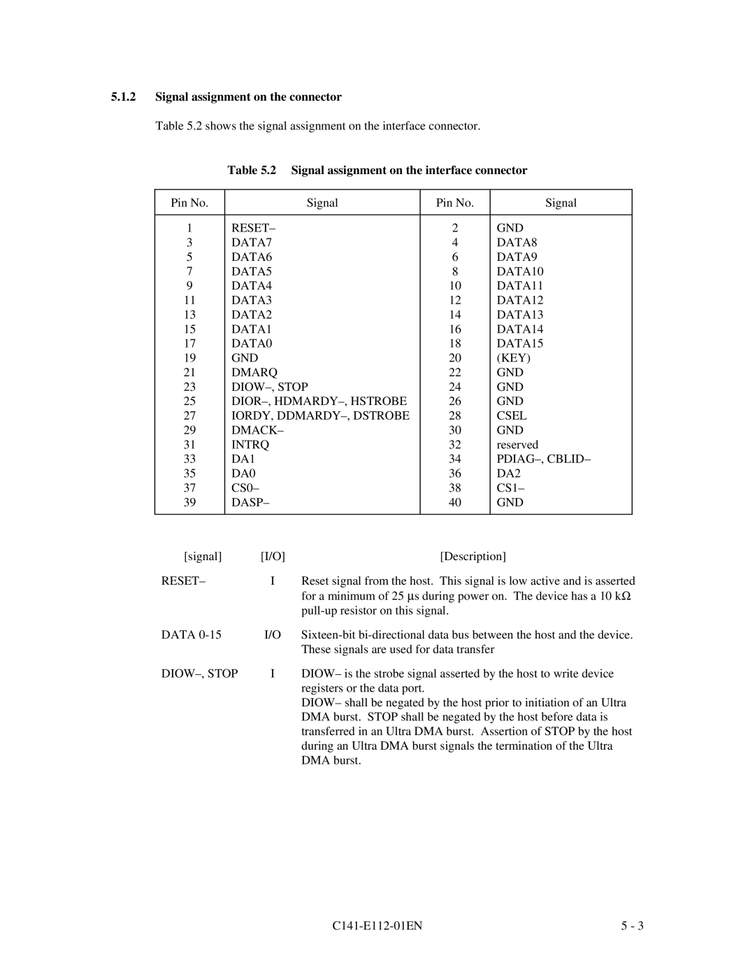
5.1.2Signal assignment on the connector
Table 5.2 shows the signal assignment on the interface connector.
Table 5.2 Signal assignment on the interface connector
Pin No. | Signal | Pin No. | Signal |
|
|
|
|
1 | RESET– | 2 | GND |
3 | DATA7 | 4 | DATA8 |
5 | DATA6 | 6 | DATA9 |
7 | DATA5 | 8 | DATA10 |
9 | DATA4 | 10 | DATA11 |
11 | DATA3 | 12 | DATA12 |
13 | DATA2 | 14 | DATA13 |
15 | DATA1 | 16 | DATA14 |
17 | DATA0 | 18 | DATA15 |
19 | GND | 20 | (KEY) |
21 | DMARQ | 22 | GND |
23 | 24 | GND | |
25 | 26 | GND | |
27 | IORDY, | 28 | CSEL |
29 | DMACK– | 30 | GND |
31 | INTRQ | 32 | reserved |
33 | DA1 | 34 |
|
35 | DA0 | 36 | DA2 |
37 | CS0– | 38 | CS1– |
39 | DASP– | 40 | GND |
|
|
|
|
[signal] | [I/O] | [Description] |
RESET– | I | Reset signal from the host. This signal is low active and is asserted |
|
| for a minimum of 25 μs during power on. The device has a 10 kΩ |
|
| |
DATA | I/O | |
|
| These signals are used for data transfer |
I | DIOW– is the strobe signal asserted by the host to write device | |
|
| registers or the data port. |
|
| DIOW– shall be negated by the host prior to initiation of an Ultra |
|
| DMA burst. STOP shall be negated by the host before data is |
|
| transferred in an Ultra DMA burst. Assertion of STOP by the host |
|
| during an Ultra DMA burst signals the termination of the Ultra |
|
| DMA burst. |
| 5 - 3 |