Hp kayak xu700 Technical Reference Manual
2000 Hewlett-Packard Company
Contents
Network Cards
Input/Output Controller Hub 2 82801BA
Assigned Device Interrupts
Graphics Cards
Rear Panel Socket Pin Layouts
MaxiLife Test Sequence and Error Messages
Contents
Conventions
Preface
Extra Information Can Be nVIDIA graphics cards
Bibliography
HP Kayak XU700 PC Workstation Overview
System Overview
Feature Description
Two ATA-100 IDE connectors for up to four IDE devices
PCI Specification
Specification
One flexible disk drive connector
Pin serial two, buffered
Package for the Minitower Models
Front and Side Views
Package for the Minitower Models
Rear View
Internal Features
HP Kayak XU700 Minitower Front Panel
HP Kayak XU700 Minitower Front Panel
HP Kayak XU700 Minitower Specifications Characteristics
Physical Characteristics
Electrical Specifications
Power Consumption and Cooling
Power outlet or use a power block with a switch
Then there is an undetected short circuit somewhere
Operating LwA = 40.5 dB
Environmental Specifications
Operating with hard disk access LwA = 41.4 dB
Operating with floppy disk access LwA = 43.2 dB
Power Saving and Ergonometry
Power Saving and Ergonometry
Full On Suspend1 Off
Power Saving and Ergonometry for APM Systems
Power Saving Modes and Resume Events for Acpi Systems
Power-On from Space-Bar
Soft Power Down
Paper-based
Access HP World Wide Web Site
Documentation
Title
Where to Find the Information
Service
Refer to LAN Refer to online
For information on On hard disk Setting up
For address, Access HP World Wide Web Site on
Guide
System Overview Documentation
System Board
IDE
System Board Overview
AGP
Architectural View
Accessory Board Slots
Accessory Board Slots
AGP Slot
PCI Slots
Yes Yes2 Yes1
PCI Slot
Reserved. Do Not change Default Setting
System Board Switches
Switch
Reserved. Do Not change Default Settings
Chipset
Memory Controller Hub
Memory Controller Hub
Feature
Cacheability controlled by processor
Power management Arbitration
MCH Interface
Support
AGP 4x Bus
Accelerated Graphics Port AGP Bus Interface
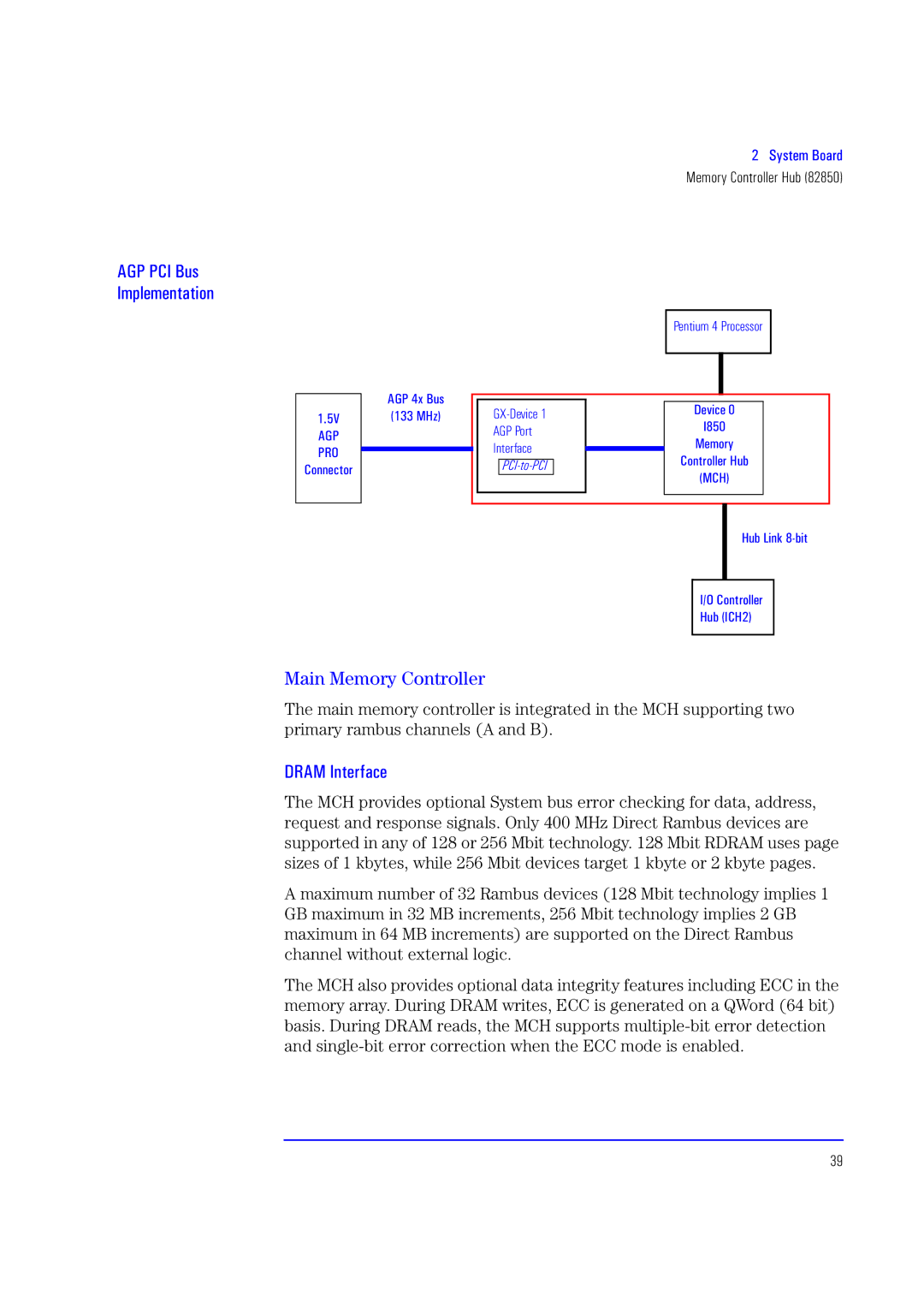
AGP PCI Bus Implementation
Main Memory Controller
Dram Interface
Dual Rambus Bus
Rimm Memory Slots
Read/Write Buffers
System Clocking
Input/Output Controller Hub 2 82801BA
Input/Output Controller Hub 2 82801BA
Following table shows the available ICH2 features
ICH2 is USB revision 1.1 compliant
Refer to the table page 59 for ICH2 interrupts
Interrupt Controller
AC’97 Controller
IDE Controller
DMA Controller
Crystal CS4299 Integrated PCI Audio
Real Time Clock Enhanced Power Management
Devices on the SMBus
Previous Architecture
PCI Bus PCI Slots
ICH2 82801AAB
Dimm Sockets
LM75 Temperature
ICH2 SMBus Master
Controller
System Board
Power cord is plugged
Following devices are connected to the LPC bus
Devices on the Low Pin Count Bus
Serial / Parallel
Be programmed as COM1, COM2, COM3, COM4, or disabled
Connector pin layouts are shown on
Super I/O Controller NS
FirmWare Hub 82802AB
Following table shows the available FWH features
FirmWare Hub 82802AB
System Bus
Voltage Regulation
Intel Pentium 4 Processor
Processor Clock
Bus Frequencies
Cache Memory
Interrupt Controllers
Assigned Device Interrupts
Input/Output Controller Hub Interrupts
PCI 64-bit Hub Interrupts
Interrupt Source
ICH2 and P64H, and allows for multiple processor operations
PCI Interrupt Request Lines
System Board Assigned Device Interrupts
Graphics Cards
Matrox Millennium G450 Graphics Card
Matrox Millennium G450 Nvidia Quadro2 MXR
3D Features
If only one monitor is used, then Port 1 must be used
To the graphics card before startup
43 / 54 aspect ratio Wide screen
Available Video Resolutions
Graphics Cards
Traditional
Wide screen
Limitations
Traditional
43 / 54 aspect ratio
Second Generation Transform and Lighting Engines
Nvidia Quadro2 MXR
HP 10/100 TX PCI LAN Interface
Network Cards
Yellow
HP 10/100 TX PCI LAN Interface Features
HP 10/100 TX PCI LAN Interface LED Descriptions
Description Flashing Steady Off
LED
Supported LAN Cards
Green
3COM LAN Card LED Descriptions
Adaptec 29160 Scsi PCI Adapter Card
Scsi Adapter Cards
Scsi Adapter Cards
Scsi Cable Information
Feature Description
Additional Scsi Card Features
IBM Deskstar
Flexible Disk Drives
Hard Disk Drives
IDE Hard Disk Drives
Quantum Atlas 10K
Scsi Hard Disk Drives
CD-ROM Drives
8X Video IDE DVD-ROM Drive
120,000 POH
Read Up to 32X 1X=150 KB/s
Write 8X CD-R 4X CD-RW
Red, Yellow, Orange, Green books
Mass Storage Devices
HP Bios
Main Screen
Using the HP Setup Program
Only if ECC modules are detected
Advanced Screen
Integrated Audio Device
PCI Device, Slot #1
Security Screen
Power Screen
Boot Screen
Updating the System Bios
Restoring Bios Default Settings
Updating the System Bios
If You Forgot the Administrator Password
If You Forgot the Administrator Password
Clearing the Cmos
Clearing the Cmos
Recovering the Bios Crisis Mode
Recovering the Bios Crisis Mode
System Memory Map
Bios Addresses
If configured
Default Values for Function Address Ports
HP I/O Port Map I/O Addresses Used by the System1
DMA controller
Default Values for Function
DMA Channel Controllers
Interrupt Controllers
Input
Interrupt Request Description
Controller and allows for multiple processor operations
Can be selected upon installation of Windows NT
There are three major interrupt modes available
Mode, only one processor executes operations
HP Bios Bios Addresses
Different diagnostics are described below
MaxiLife Test Sequence and Error Messages
MaxiLife Test Sequence and Error Messages
Basic Pre-boot Diagnostics
Pre-boot Diagnostics Error Codes
Test Error Code Beep Codes Action to Take
Number Problem
Post Test Sequence and Post Error
Following diagrams show the different BIOS-generated errors
100
Run-Time Errors
Operating System Boot Phase
Main Menu Minitower models only
Test Error Code Action to Take
Boot Steps
Boot report
System Info
104
Order in Which Post Tests Are Performed
Beep
Post Routine Description
Codes
Check video configuration against Cmos
Enable cache before system Bios shadow
Shadow system Bios ROM Shadow Bios
Advanced configuration of chipset registers
Disable CPU cache
Enable keyboard
Initialize Post display service
Display prompt Press F2 to enter Setup
Initialize Extended Bios Data Area
Detect and install external parallel ports
Initialize Bios Data Area
Enable Non-Maskable Interrupts NMIs
Terminate QuietBoot optional
Enter Setup
Clear Boot flag
Check for errors Checking
Go to Bios
Initialize system timer
Check force recovery boot
Checksum Bios ROM
Boot to Full DOS
Initialize System Management Mode
Output one beep before boot
Boot to Mini DOS
Error Message Summary
Error Message Summary
113
Cause / Symptom
Message
116
Other
Battery Pinouts
IDE Drive Connectors
Rear Fan Connector
Additional Scsi LED Connector
Aux Power Connector
Wake On LAN Connector
Status Panel Intrusion
Internal Audio Connectors
LCD Panel
Hard Disk Drive Temperature Connector
VGA DB15 Connector
Video Connector
121
Ethernet UTP Connector
Keyboard and Mouse Connectors
Keyboard and Mouse Connectors Pin Signal
Rear Panel Socket Pin Layouts
Pin Serial Port Connector Signal
USB Connector
MIDI/Joystick Connector Pin Signal
Pin Parallel Connector
MIDI/Joystick Connector
Pin Parallel Connector Signal