FUNCTIONAL | DESCRIPTION |
III. 16550 FUNCTIONAL | DESCRIPTION |
T h e 1 6 5 5 0 i s a n u p g r a d e o f t h e s t a n d a r d 1 6 4 5 0 | |
Asynchronous Communications | Element (ACE). Designed to |
b e c o m p a t i b l e w i t h t h e 1 6 4 5 0 , t h e 1 6 5 5 0 e n t e r s t h e character mode on reset and in this mode will appear as a 16450 to user software. An additional mode, FIFO mode,
c a n b e s e l e c t e d | t o r e d u c e C P U o v e r h e a d a t h i g h d a t a |
rates. The FIFO | mode increases performance by providing |
two | internal | |||
to | buffer data | and | reduce | the number of interrupts issued |
to | the CPU. |
|
|
|
Other features of | the | 16550 | include: | |
| Programmable baud rate, character length, parity, | |||
and number of stop bits |
| |||
| Automatic addition and removal of start, stop, and | |||
parity bits |
|
|
| |
| Independent and prioritized transmit, receive and | |||
status interrupts |
|
|
| |
| Transmitter clock output to drive receiver logic | |||
| External receiver | clock | input | |
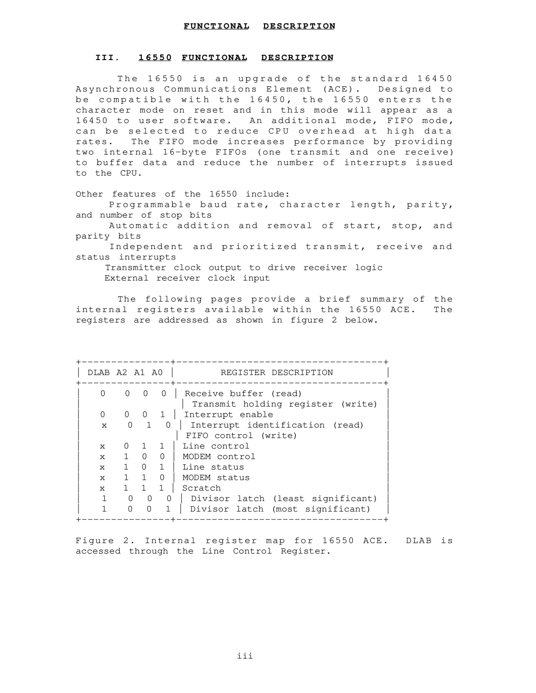
The following pages provide a brief summary of the internal registers available within the 16550 ACE. The registers are addressed as shown in figure 2 below.
+ |
|
|
|
|
| + | |||||
DLAB | A2 | A1 | A0 | REGISTER | DESCRIPTION | ||||||
+ |
|
|
|
|
| + | |||||
0 | 0 | 0 | 0 | Receive buffer | (read) |
| |||||
|
|
|
|
| Transmit holding register (write) | ||||||
0 | 0 | 0 | 1 | Interrupt | enable |
| |||||
x | 0 | 1 | 0 | Interrupt identification (read) | |||||||
|
|
|
|
| FIFO control (write) |
| |||||
x | 0 | 1 | 1 Line control |
|
| ||||||
x | 1 | 0 | 0 MODEM control |
|
| ||||||
x | 1 | 0 | 1 Line status |
|
| ||||||
x | 1 | 1 | 0 MODEM status |
|
| ||||||
x | 1 | 1 | 1 Scratch |
|
|
| |||||
1 | 0 | 0 |
| 0 | Divisor | latch | (least | significant) | |||
1 | 0 | 0 |
| 1 | Divisor | latch | (most | significant) | |||
+ |
|
|
|
|
| + | |||||
