82540EP — Networking Silicon
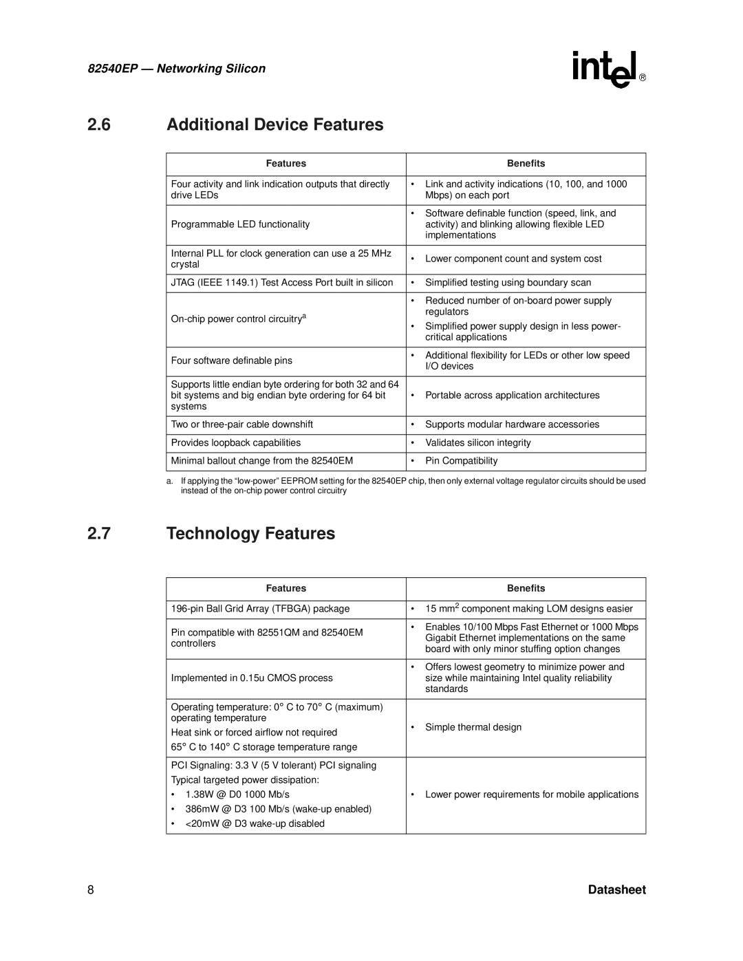
2.6 | Additional Device Features |
|
|
|
|
|
|
| Features |
| Benefits |
|
|
| |
| Four activity and link indication outputs that directly | • Link and activity indications (10, 100, and 1000 | |
| drive LEDs |
| Mbps) on each port |
|
|
| |
|
| • Software definable function (speed, link, and | |
| Programmable LED functionality |
| activity) and blinking allowing flexible LED |
|
|
| implementations |
|
|
|
|
| Internal PLL for clock generation can use a 25 MHz | • Lower component count and system cost | |
| crystal | ||
|
|
| |
|
|
| |
| JTAG (IEEE 1149.1) Test Access Port built in silicon | • Simplified testing using boundary scan | |
|
|
| |
|
| • Reduced number of | |
|
| regulators | |
| • Simplified power supply design in less power- | ||
|
| ||
|
|
| critical applications |
|
|
| |
| Four software definable pins | • Additional flexibility for LEDs or other low speed | |
|
| I/O devices | |
|
|
| |
|
|
|
|
| Supports little endian byte ordering for both 32 and 64 |
|
|
| bit systems and big endian byte ordering for 64 bit | • | Portable across application architectures |
| systems |
|
|
|
|
|
|
| Two or | • | Supports modular hardware accessories |
|
|
|
|
| Provides loopback capabilities | • | Validates silicon integrity |
|
|
|
|
| Minimal ballout change from the 82540EM | • | Pin Compatibility |
|
|
|
|
a.If applying the
2.7Technology Features
Features |
| Benefits | |
|
|
| |
• | 15 mm2 component making LOM designs easier | ||
Pin compatible with 82551QM and 82540EM | • Enables 10/100 Mbps Fast Ethernet or 1000 Mbps | ||
| Gigabit Ethernet implementations on the same | ||
controllers |
| ||
| board with only minor stuffing option changes | ||
|
| ||
|
| ||
| • Offers lowest geometry to minimize power and | ||
Implemented in 0.15u CMOS process |
| size while maintaining Intel quality reliability | |
|
| standards | |
|
|
| |
Operating temperature: 0° C to 70° C (maximum) |
|
| |
operating temperature | • | Simple thermal design | |
Heat sink or forced airflow not required | |||
|
| ||
65° C to 140° C storage temperature range |
|
| |
|
|
| |
PCI Signaling: 3.3 V (5 V tolerant) PCI signaling |
|
| |
Typical targeted power dissipation: |
|
| |
• 1.38W @ D0 1000 Mb/s | • | Lower power requirements for mobile applications | |
• 386mW @ D3 100 Mb/s |
|
| |
• <20mW @ D3 |
|
| |
|
|
| |
8 | Datasheet |