Networking Silicon — 82540EP
3.0Signal Descriptions
Note: The targeted signal names are subject to change without notice. Verify with your local Intel sales office that you have the latest information before finalizing a design.
3.1Signal Type Definitions
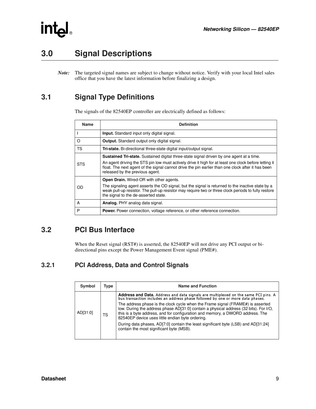
The signals of the 82540EP controller are electrically defined as follows:
Name | Definition | |
|
| |
I | Input. Standard input only digital signal. | |
|
| |
O | Output. Standard output only digital signal. | |
|
| |
TS | ||
|
| |
| Sustained | |
STS | An agent driving the STS pin low must actively drive it high for at least one clock before letting it | |
float. The next agent of the signal cannot drive the pin earlier than one clock after it has been | ||
| ||
| released by the previous agent. | |
|
| |
| Open Drain. | |
OD | The signaling agent asserts the OD signal, but the signal is returned to the inactive state by a | |
weak | ||
| ||
| the signal to the | |
|
| |
A | Analog. PHY analog data signal. | |
|
| |
P | Power. Power connection, voltage reference, or other reference connection. | |
|
|
3.2PCI Bus Interface
When the Reset signal (RST#) is asserted, the 82540EP will not drive any PCI output or bi- directional pins except the Power Management Event signal (PME#).
3.2.1PCI Address, Data and Control Signals
Symbol | Type | Name and Function |
|
|
|
|
| Address and Data. |
|
| The address phase is the clock cycle when the Frame signal (FRAME#) is asserted |
AD[31:0] |
| low. During the address phase AD[31:0] contain physical address (32 bits). For I/O, |
| this is byte address, and for configuration and memory, a DWORD address. The | |
| TS | 82540EPbustransactiondeviceincludesusesAddresslittleanendianaddressanddatabytephasesignalsordering.followedaremultiplexedbyoneormoreonthedatasamephasesPCIpins..A |
|
| During data phases, AD[7:0] contain the least significant byte (LSB) and AD[31:24] |
|
| contain the most significant byte (MSB). |
|
|
|
Datasheet | 9 |
