82540EP — Networking Silicon
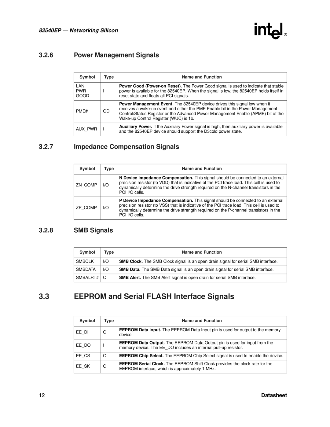
3.2.6Power Management Signals
Symbol | Type | Name and Function | |
|
|
| |
LAN_ |
| Power Good | |
PWR_ | I | power is available for the 82540EP. When the signal is low, the 82540EP holds itself in | |
GOOD |
| reset state and floats all PCI signals. | |
|
|
| |
|
| Power Management Event. The 82540EP device drives this signal low when it | |
PME# | OD | receives a | |
Control/Status Register or the Advanced Power Management Enable (APME) bit of the | |||
|
| ||
|
| ||
|
|
| |
AUX_PWR | I | Auxiliary Power. If the Auxiliary Power signal is high, then auxiliary power is available | |
and the 82540EP device should support the D3cold power state. | |||
|
| ||
|
|
|
3.2.7Impedance Compensation Signals
Symbol | Type | Name and Function | |
|
|
| |
|
| N Device Impedance Compensation. This signal should be connected to an external | |
ZN_COMP | I/O | precision resistor (to VDD) that is indicative of the PCI trace load. This cell is used to | |
dynamically determine the drive strength required on the | |||
|
| ||
|
| PCI I/O cells. | |
|
|
| |
|
| P Device Impedance Compensation. This signal should be connected to an external | |
ZP_COMP | I/O | precision resistor (to VSS) that is indicative of the PCI trace load. This cell is used to | |
dynamically determine the drive strength required on the | |||
|
| ||
|
| PCI I/O cells. | |
|
|
|
3.2.8SMB Signals
Symbol | Type | Name and Function |
|
|
|
SMBCLK | I/O | SMB Clock. The SMB Clock signal is an open drain signal for serial SMB interface. |
|
|
|
SMBDATA | I/O | SMB Data. The SMB Data signal is an open drain signal for serial SMB interface. |
|
|
|
SMBALRT# | O | SMB Alert. The SMB Alert signal is open drain for serial SMB interface. |
|
|
|
3.3EEPROM and Serial FLASH Interface Signals
Symbol | Type | Name and Function | |
|
|
| |
EE_DI | O | EEPROM Data Input. The EEPROM Data Input pin is used for output to the memory | |
device. | |||
|
| ||
|
|
| |
EE_DO | I | EEPROM Data Output. The EEPROM Data Output pin is used for input from the | |
memory device. The EE_DO includes an internal | |||
|
| ||
|
|
| |
EE_CS | O | EEPROM Chip Select. The EEPROM Chip Select signal is used to enable the device. | |
|
|
| |
EE_SK | O | EEPROM Serial Clock. The EEPROM Shift Clock provides the clock rate for the | |
EEPROM interface, which is approximately 1 MHz. | |||
|
| ||
|
|
|
12 | Datasheet |
