82540EP — Networking Silicon
Symbol | Type |
| Name and Function | |||
|
|
| ||||
|
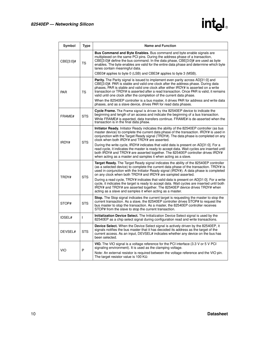
| Bus Command and Byte Enables. Bus command and byte enable signals are | ||||
|
| multiplexed on the same PCI pins. During the address phase of a transaction, | ||||
CBE[3:0]# | TS | CBE[3:0]# define the bus command. In the data phase, CBE[3:0]# are used as byte | ||||
| enables. The byte enables are valid for the entire data phase and determine which byte | |||||
|
| |||||
|
| lanes contain meaningful data. |
|
| ||
|
| CBE0# applies to byte 0 (LSB) and CBE3# applies to byte 3 (MSB). | ||||
|
|
| ||||
|
| Parity. The Parity signal is issued to implement even parity across AD[31:0] and | ||||
|
| CBE[3:0]#. PAR is stable and valid one clock after the address phase. During data | ||||
|
| phases, PAR is stable and valid one clock after either IRDY# is asserted on a write | ||||
PAR | TS | transaction or TRDY# is asserted after a read transaction. Once PAR is valid, it remains | ||||
|
| valid until one clock after the completion of the current data phase. | ||||
|
| When the 82540EP controller is a bus master, it drives PAR for address and write data | ||||
|
| phases, and as a slave device, drives PAR for read data phases. | ||||
|
|
|
|
|
| |
|
| Cycle Frame. | TheFramesignalis |
| 82540EP device to indicate the | |
|
|
|
| bythe | ||
FRAME# | STS | beginning and length of an access and indicate the beginning of a bus transaction. | ||||
|
| While FRAME# is asserted, data transfers continue. FRAME# is | ||||
|
| transaction is in the final data phas |
|
| ||
|
| Initiator Ready. Initiator Ready indicates the ability of the 82540EP controller (as bus | ||||
|
| master device) to complete the current data phase of the transaction. IRDY# is used in | ||||
|
| conjunction with the Target Ready signal (TRDY#). The data phase is completed on any | ||||
IRDY# | STS | clock when both IRDY# and TRDY# are asserted. | ||||
|
| . |
| |||
|
| During the write cycle, IRDY# indicates that valid data is present on AD[31:0]. For a | ||||
|
| read cycle, it indicates the master is ready to accept data. Wait cycles are inserted until | ||||
|
| both IRDY# and TRDY# are asserted together. The 82540EP controller drives IRDY# | ||||
|
| when acting as a master and samples it when acting as a slave. | ||||
|
| Target Ready. | Target Ready signal indicates the ability of the 82540EP controller | |||
|
| (as a selected device) to complete the current data phase of the transaction. TRDY# is | ||||
|
| used in conjunction with the Initiator Ready signal (IRDY#). A data phase is completed | ||||
TRDY# | STS | on any clock when both TRDY# and IRDY# are sampled asserted. | ||||
During a read cycle, TRDY# indicates that valid data is present on AD[31:0]. For a write | ||||||
|
| |||||
|
| cycle, it indicates the target is ready to accept data. Wait cycles are inserted until both | ||||
|
| IRDY# and TRDY# are asserted together. The 82540EP device drives TRDY# when | ||||
|
| acting as a slave and samples it when acting as a master. | ||||
|
|
| ||||
|
| Stop. The Stop signal indicates the current target is requesting the master to stop the | ||||
STOP# | STS | current transaction. As slave, the 82540EP controller drives STOP# to request the | ||||
bus master to stop the transaction. As a master, the 82540EP controller receives | ||||||
|
| |||||
|
| STOP# from the slave to stop the current transaction. | ||||
|
|
| ||||
IDSEL# | I | Initialization Device Select. The Initialization Device Select signal is used by the | ||||
82540EP as a chip select signal during configuration read and write transactions. | ||||||
|
| |||||
|
| driven | ||||
|
| Device Select. When the Device Select signal is actively driven by the 82540EP, it | ||||
DEVSEL# | STS | signals notifies the bus master that it has decoded its address as the target of the | ||||
current access. As an input, DEVSEL# indicates whether any device on the bus has | ||||||
|
| |||||
|
| been selected. |
|
|
| |
|
|
| ||||
|
| VIO. The VIO signal is a voltage reference for the PCI interface (3.3 V or 5 V PCI | ||||
VIO | P | signaling environment). It is used as the clamping voltage. | ||||
Note: An external resistor is required between the voltage reference and the VIO pin. | ||||||
|
| |||||
|
| The target resistor value is 100 KΩ |
|
| ||
|
|
|
|
|
| |
10 | Datasheet |
