MD566X
Revision History
Acronym Definition
Symbol Units of measure
Conventions
Programmer’s Guide
Dram
Introduction
Chipset Contents Qty
Intel V.90/V.92 56K Chipsets
Modem Connection Overview
V.92, V.90 and V.34 Data Modes
DCE-to-DCE Data Rates for Each Mode
DTE-to-DCE Data Rates for Each Mode
Mode Data Rate bps Affected Data
Data Mode Command Summary
AT Command Summary Tables
Command Function Default Range Reported by
Intel Confidential
Data rate Result code type Yes
Ports only Async mode
+GMI?
Intel Confidential
Command Function Default Range Reported By &Vn
V.44 / V.42 / V.42 bis MNP∗ Command Summary
Intel Confidential
Value saved in Nvram
Fax Class 1 Command Summary
Fax Identity Command Summary
IS-101 Voice Command Summary
Response Hex Code Function
Voice DTE→DCE Character Pairs
Voice DTE←DCE Character Pairs
Register Function Default Range Units Reported By &Vn
Dial Modifiers Command Function
S-Register Summary
Verbose Code Numeric Code
10. V.90/V.92 Mode DCE-to-ISP Response Codes
12. DTE-to-DCE Data Rate Response Codes
11. V.34 Mode DCE-to-DCE Response Codes
Command Function Default Range
13. Manufacturing-Only Command Summary a
Modem Setup Host Command Modem Response
Basic Data Mode AT Commands
Using AT Commands to Access the S-Registers Sn?, Sn=x, ?
Modem Responses and Command Echo En, Vn, Xn, Wn, Qn
Example of a Remote Connection
Information
Product Identification Information
Establishing a Modem Connection A, D, DS = n, S0
Hanging Up Hn, S10, Zn, &D2
Online Command Mode Escape Codes, On
Modem-to-Modem Connection Data Rates
Intel Confidential
Intel Confidential
ATH +PMHF
+PMHR
Carrier Description
Supported Modulation Types
S37
+MS = carrier , automode, min rate, max rate
Figured to attempt only a 28,800 bps connec
Originating Answering Resulting Connection Speed Modem
Local Analog Loopback AT&T1
Diagnostic Testing S18, &Tn
AT&T0
Local Analog Loopback with Self-Test
Local Analog Loopback With Self-Test AT&T8
Licensing Requirements for Hayes Escape Sequence
AT Escape Sequences
Time-Independent Escape Sequence
Hayes∗ Escape Sequence
Command Default Description
Data Mode Command Descriptions
None
Stant carrier mode
Dialing Digits
Online data mode echo
Reports product code
ATI5
Cont
Mode from online command mode
Sn?
Sn=x
Protocol Lapm
Sequent commands to be ignored
For data mode
Ports asynchronous mode. This command is the same as &M0
User profile n
Zn=x None
Modem power-up
+GMR?
V34BS
+MS=m See m
Cont
Modulation Selection
+MS=m
Examples DTE data rate = 115,200 bps
Examples DTE data rate = 2400 bps
+PMH=m
+PCW=m
DCE
+PMHR none
Mand
+PSS=m
Intel Confidential
Mode Features
Error Correction and Data Compression
Resulting \Nn Connection Types
Bis with fallback to MNP5 \N3
\Bn None
\An
\Gn
\Cn
\Jn
\Nn
\Kn
\Tn
\Qn
\Xn
Intel Confidential
+DS44=m 972,140
0,471
140,1884 3768
Tocols
FAX Class 1 AT Commands
Fax Identity Commands
Fax Identity Command Descriptions
+FREV?/+FMR? none
Fax Class 1 Commands
Value Modulation Speed Bps
Mod Selection Table
Class 1 DTE-Generated Hdlc Frame Information AT+FTH=mod
+FCLASS=1
Fax Mode Command Descriptions
+FRS=n None
Command Default Description Receive Hdlc Data
+FRH=n
+FRM=n None
DTE after receiving the +FTH=mod command
Data using the modulation selected in mod
Each command may be used as follows
IS-101 Voice Mode AT Commands
Relay Control
Dtmf Detection
+FLO=n
Voice Mode Command Descriptions
+VCID=n
+VBT=m
+VDR=m
Enable Report Function
+VEM=m See m
Dialtone
+VEM=m
Example 1. Viewing Supported Events
Example 2. Setting the Event Mask
Example 3. Reading the Event Mask Settings
Event Reporting and Masking
+VGT=n
+VGM=n 128
+VGR=n 128
+VGS=n
+VIP none
+VLS=n
Code
Primitive Code +VLS=n
Relay/Playback Control
+VNH=n
Intel Confidential
+VRX none
+VSD=m See ‘m’
= sds, sdi Defaults m = 128
Vsr Comments Samples/second
Manufac +VSM=m turer- specified
Hard Disk
Compression Method Selection
+VSM=m Manufac
Vsr
+VTD=n 100
+VSP=n
+VTS=m none
AT+VTS=DTMF or
Dtmf and Tone Generation
AT+VTS= , ,duration For example AT+VTS= , ,50
Intel Confidential
Registers
S-Register Command Descriptions
Ascii decimal
S11
S10
S12
S16
S14 138
S22 118
S21
S27
S23 None
S31
S33
Maximum Line Speed Attempted
110
Caller ID Tags for Formatted Reporting
Caller ID
Ring
Manufacturing-Only Command Descriptions
MANUFACTURING-ONLY Commands
NCnn
S92
S91
$TTnn
FAX Test
Tone Test Command Analog Loopback ALB Test
#VGP2=n
Command Bit Pins
#VGP0=n
#VGP1=n See Note
118
Programmer’s Guide
Parallel Host Interface 16C450/16C550A Uart
119
Register BIT Number Address Name
Parallel Host Interface Uart Register Bit Assignments
Line Status Register LSR
Uart Register Definitions
Scratch Register SCR
Modem Status Register MSR
Modem Control Register MCR
Are no subsequent Fifo errors
123
Line Control Register LCR
Trigger Level Bytes
Fifo Control Register FCR
Interrupt Control Functions
Interrupt Identity Register IIR
125
Transmitter Holding Register THR
Interrupt Enable Register IER
10.1.10Receiver Buffer Register RBR
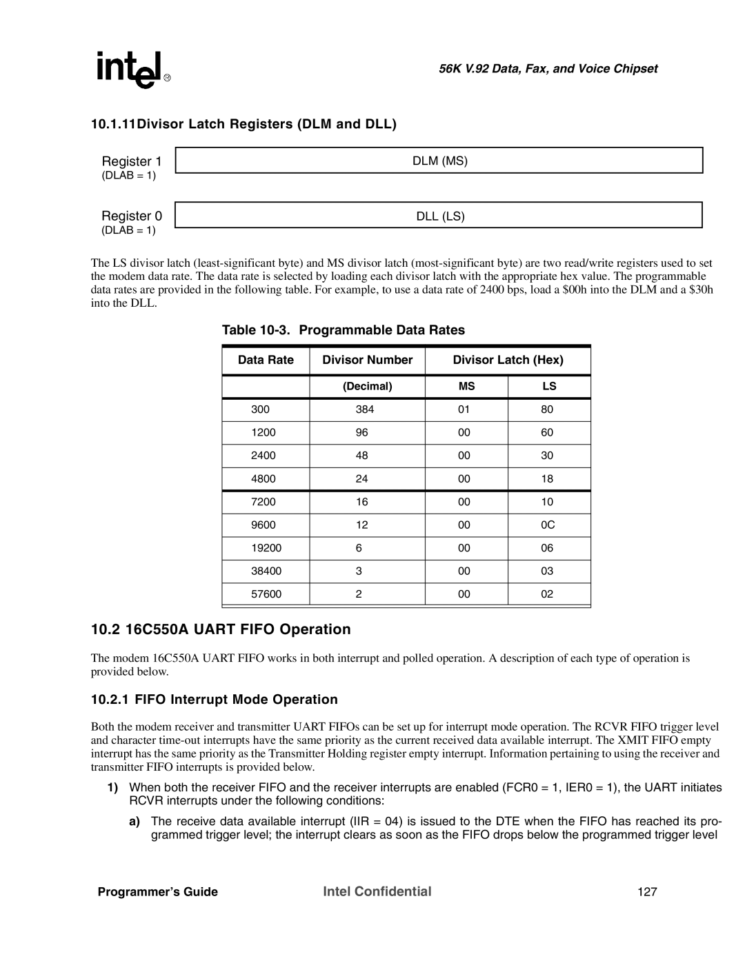
Programmable Data Rates
Fifo Interrupt Mode Operation
10.2 16C550A Uart Fifo Operation
10.1.11Divisor Latch Registers DLM and DLL
Fifo Polled Mode Operation
129
130