SP200/210 | Maxon SP200/210 Radio |
Battery Low Indicator Circuit
When the battery voltage drops below 5.6 VDC a Battery Low indication is given. Due to the volts drop across D403, a voltage below 5.6V on the battery gives a voltage less than 5V on the base of Q405. , Q405 switches on its when base is below 5v (current flow through R413), which switches on Q404, so driving pin 52 of the microcontroller low (normally tied high). The micro controller disables the transmitter and at the same time enables the red LED and sends an alert tone to warn the user. The battery should be replaced or recharged at this time (one transmission is allowed after the low battery warning).
LEDs and indicators
The red and green LEDs are switched on, via Q407and Q411, by control lines from the microcontroller. Both the red and green LEDs being lit indicate the condition ‘busy’ i.e. orange. Both the LCD and backlight are driven from the microcontroller.
The alert tones are generated in the microcontroller and are fed through a filter to the volume control via link 27. There is an option of routing the tones directly to the audio amp via link28.
5.5 Common RF Circuits
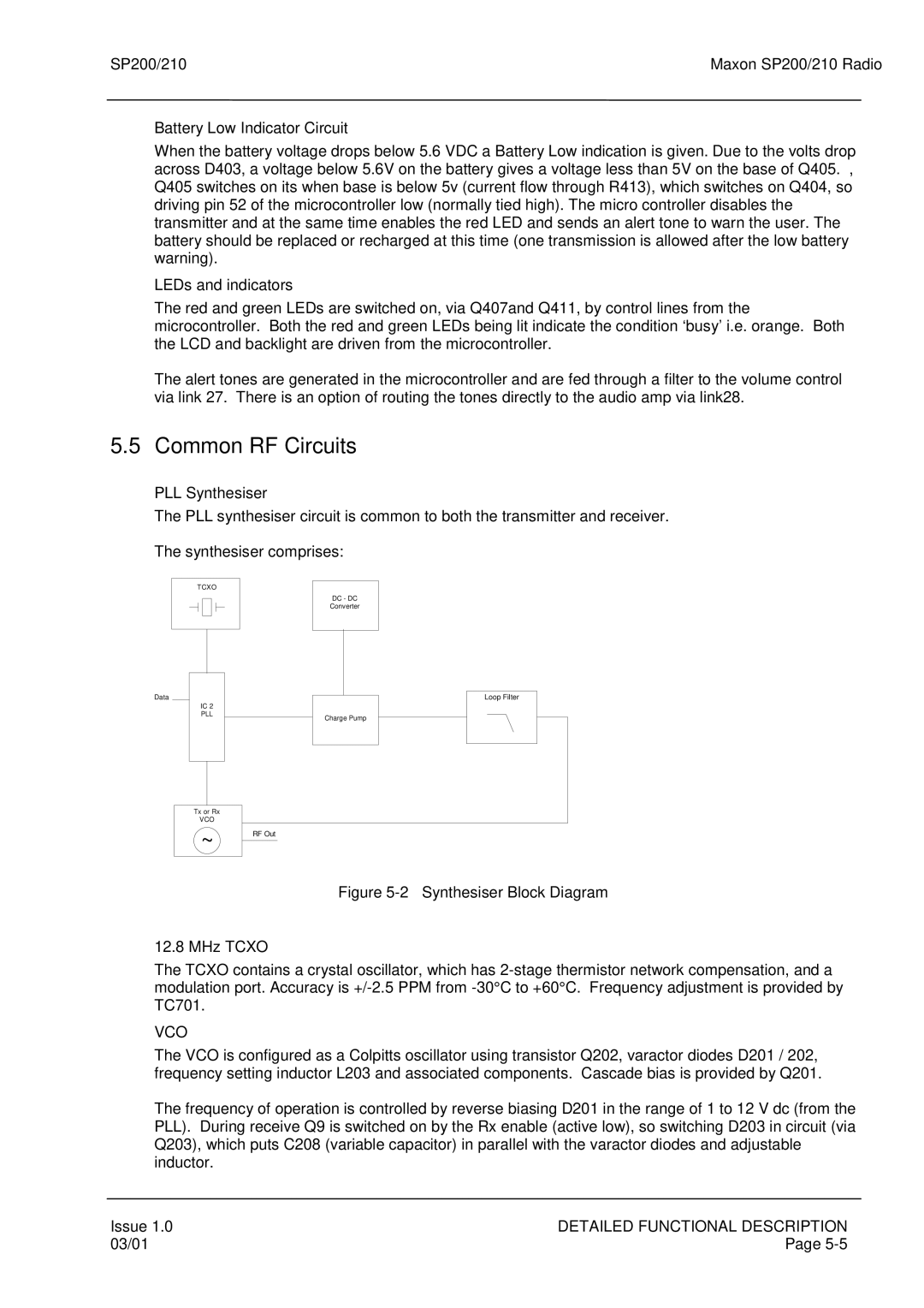
PLL Synthesiser
The PLL synthesiser circuit is common to both the transmitter and receiver.
The synthesiser comprises:
TCXO
DC - DC
Converter
Data
IC 2 |
|
PLL | Charge Pump |
|
Loop Filter
Tx or Rx
VCO
~
RF Out
Figure 5-2 – Synthesiser Block Diagram
12.8 MHz TCXO
The TCXO contains a crystal oscillator, which has
VCO
The VCO is configured as a Colpitts oscillator using transistor Q202, varactor diodes D201 / 202, frequency setting inductor L203 and associated components. Cascade bias is provided by Q201.
The frequency of operation is controlled by reverse biasing D201 in the range of 1 to 12 V dc (from the PLL). During receive Q9 is switched on by the Rx enable (active low), so switching D203 in circuit (via Q203), which puts C208 (variable capacitor) in parallel with the varactor diodes and adjustable inductor.
Issue 1.0 | DETAILED FUNCTIONAL DESCRIPTION |
03/01 | Page |