Maxon SP200/210 Radio | SP200/210 |
5.7 Receiver
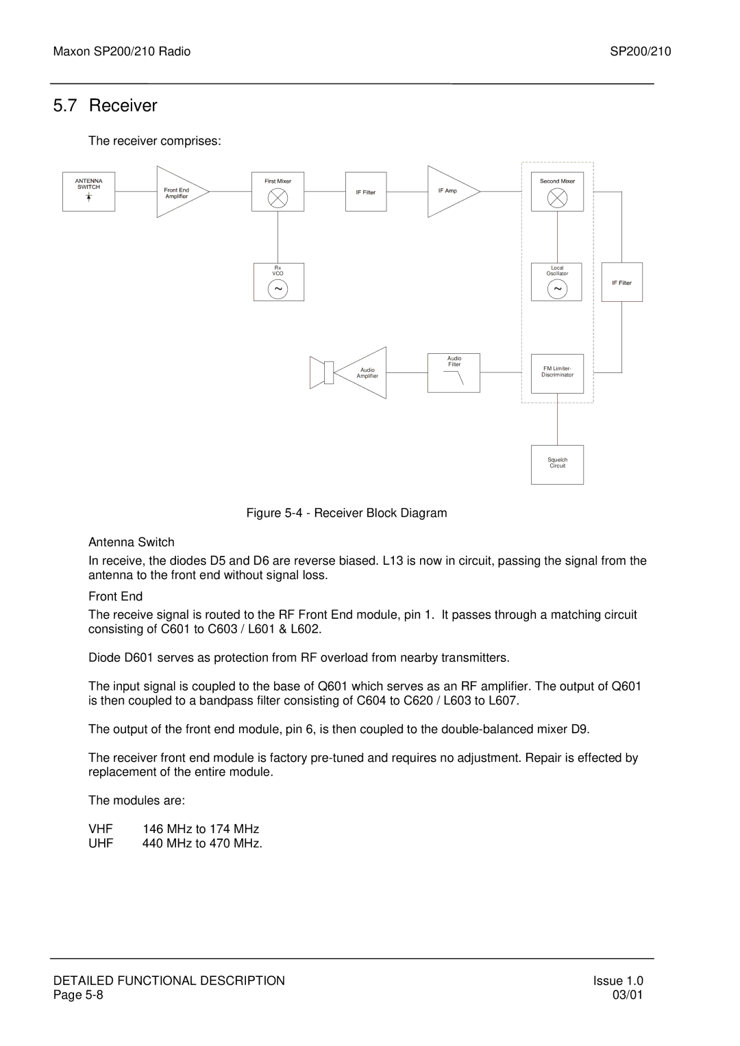
The receiver comprises:
Rx
VCO
~
Audio
Amplifier
Audio
Filter
Local
Oscillator
~
FM Limiter- Discriminator
Squelch
Circuit
Figure 5-4 - Receiver Block Diagram
Antenna Switch
In receive, the diodes D5 and D6 are reverse biased. L13 is now in circuit, passing the signal from the antenna to the front end without signal loss.
Front End
The receive signal is routed to the RF Front End module, pin 1. It passes through a matching circuit consisting of C601 to C603 / L601 & L602.
Diode D601 serves as protection from RF overload from nearby transmitters.
The input signal is coupled to the base of Q601 which serves as an RF amplifier. The output of Q601 is then coupled to a bandpass filter consisting of C604 to C620 / L603 to L607.
The output of the front end module, pin 6, is then coupled to the
The receiver front end module is factory
The modules are:
VHF | 146 MHz to 174 MHz |
UHF | 440 MHz to 470 MHz. |
DETAILED FUNCTIONAL DESCRIPTION | Issue 1.0 |
Page | 03/01 |