Manuals
/
Brands
/
Communications
/
Two-Way Radio
/
Maxon Telecom
/
Communications
/
Two-Way Radio
Maxon Telecom
SP200, SP210
- page 46
1
46
95
95
Download
95 pages, 3.03 Mb
Ma
x
on S
P2
0
0/210
Ra
d
i
o
S
P2
0
0
/210
T
R
O
U
BLESH
OO
T
ING
I
ss
ue 1.0
Page 6-8
03/01
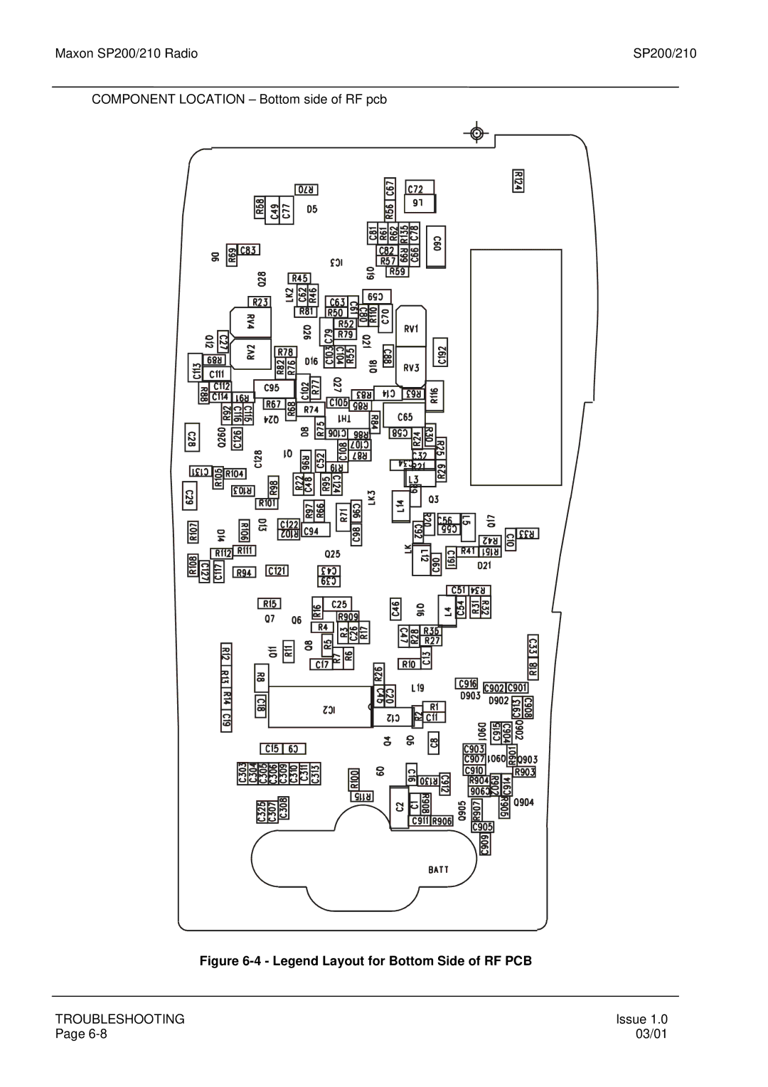
COMPONENT LOCATION – Bottom side of RF pcb
Figure 6-4 - Legend Layout for Bottom Side of RF PCB
Contents
Main
Page
Page
Page
TABLE OF CONTENTS
1 INTRODUCTION 1-1
2 SPECIFICATIONS 2-1
3 ACCESSORIES & OPTIONS 3-1
4 INSTALLATION, COMMISSIONING & ALIGNMENT 4-1
8 EXPLODED MECHANICAL DRAWINGS & PARTS LISTS 8-1
9 CIRCUIT DIAGRAMS & PCB LAYOUTS 9-1 10 SPARE PARTS 10-1
11 APPENDIX ACC-2003 ALIGNMENT BOX 11-1
LIST OF FIGURES
LIST OF TABLES
Page
1 INTRODUCTION
1.1 Using this Manual
1.2 Amendments to this Manual
1.3 Contact Information
2 SPECIFICATIONS
2.1 General
Page
3 ACCESSORIES & OPTIONS
3.1 Pre-Install Check
3.2 Accessories
3.3 Options
Page
4 INSTALLATION, COMMISSIONING & ALIGNMENT
4.1 Installation
11
12
4.2 Connections
4.3 Commissioning
Page
Page
Page
4.3.1 Test Equipment Connection
4.3.2 Transmitter Performance Tests
4.3.3 Receiver Performance Tests
4.4 Power Adjustment
PowerSquelch
4.5 Alignment
4.5.1 Preparation
4.5.2 Disassembly and Re-assembly of the Radio
RF PCB
4.5.3 PLL Alignment
4.5.4 Squelch Sensitivity
4.5.5 Transmitter Alignment
RADIOCOMMUNICATIONS TEST SET
Page
4.5.6 Receiver Alignment
5 DETAILED FUNCTIONAL DESCRIPTION
5.1 Introduction
5.2 Common Circuits
5.3 Audio ASIC
5.3.1 Audio Signal Path
5.3.2 Sat Signal Path
5.3.3 Miscellaneous Signals and Controller
5.4 Audio/SAT Circuits
5.5 Common RF Circuits
~
Page
5.6 Transmitter
5.7 Receiver
~
Page
Page
6 TROUBLESHOOTING
6.1 Diagnostic Function
6.2 Troubleshooting Chart
6.3 Voltage Charts
6.3.1 Transistors (Main Circuit)
Maxon SP200/210 Radio SP200/210
TROUBLESHOOTING Issue 1.0 Page 6-4 03/01
6.3.2 Integrated Circuits
Table 6-5 - Integrated Circuit Voltages (Transmit)
Receive
Table 6-4 - Integrated Circuit Voltages (Receive) Transmit
Page
Page
Page
Page
7 PROGRAMMING
7.1 SMP6100
7.1.1 Introduction
7.1.2 Getting Started
7.1.3 Programming
Page
Page
Page
8 EXPLODED MECHANICAL DRAWINGS & PARTS LISTS
8.1 Parts List
8.2 Spare Parts
Page
Page
Page
Page
Page
Page
8.4 SL100 VHF Parts List
8.4.1 V2 Control Circuit
Page
8.4.2 V2 RF
Page
Page
8.4.3 TCXO Assembly
8.4.4 V2 VCO
8.4.5 V2 Front End
8.5 SL100 UHF Parts List
8.5.1 U2 Contr o l Circuit
Page
8.5.2 U2 RF
Page
Page
8.5.3 TCXO
8.5.4 VCO
Page
9 CIRCUIT DIAGRAMS & PCB LAYOUTS
Page
Page
Page
Page
Page
Page
Page
10 SPARE PARTS
10.1 Spare Parts
10.1.1 Component Replacement
Page
Page
11 APPENDIX ACC-2003 ALIGNMENT BOX
11.1 Purpose
11.2 Test Equipment
11.3 Calibration Program
11.3.1 Operation
Page
Page
11.3.2 Adjustment of ASIC values
Page
11.3.3 Transmit Adjustments
11.3.4 Receive Adjustments
11.4 Default Settings
11.4.1 V1 Band Default Settings
11.4.2 V2 Band Default Settings
11.4.3 U1 Band Default Settings
11.4.4 U2 Band Default Settings