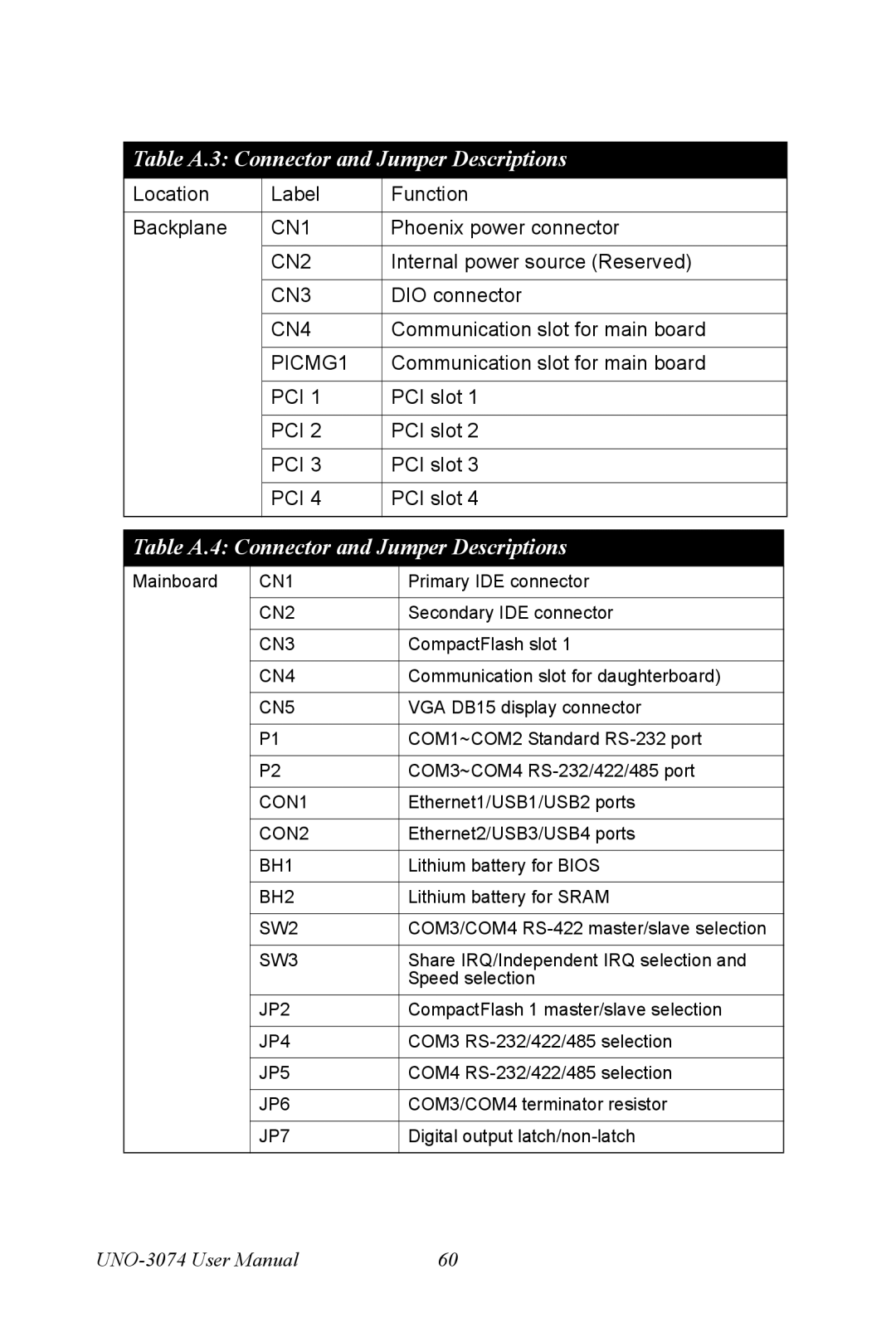
Table A.3: Connector and Jumper Descriptions
Location | Label | Function |
|
|
|
Backplane | CN1 | Phoenix power connector |
|
|
|
| CN2 | Internal power source (Reserved) |
|
|
|
| CN3 | DIO connector |
|
|
|
| CN4 | Communication slot for main board |
|
|
|
| PICMG1 | Communication slot for main board |
|
|
|
| PCI 1 | PCI slot 1 |
|
|
|
| PCI 2 | PCI slot 2 |
|
|
|
| PCI 3 | PCI slot 3 |
|
|
|
| PCI 4 | PCI slot 4 |
|
|
|
Table A.4: Connector and Jumper Descriptions
Mainboard | CN1 | Primary IDE connector |
|
|
|
| CN2 | Secondary IDE connector |
|
|
|
| CN3 | CompactFlash slot 1 |
|
|
|
| CN4 | Communication slot for daughterboard) |
|
|
|
| CN5 | VGA DB15 display connector |
|
|
|
| P1 | COM1~COM2 Standard |
|
|
|
| P2 | COM3~COM4 |
|
|
|
| CON1 | Ethernet1/USB1/USB2 ports |
|
|
|
| CON2 | Ethernet2/USB3/USB4 ports |
|
|
|
| BH1 | Lithium battery for BIOS |
|
|
|
| BH2 | Lithium battery for SRAM |
|
|
|
| SW2 | COM3/COM4 |
|
|
|
| SW3 | Share IRQ/Independent IRQ selection and |
|
| Speed selection |
| JP2 | CompactFlash 1 master/slave selection |
|
|
|
| JP4 | COM3 |
|
|
|
| JP5 | COM4 |
|
|
|
| JP6 | COM3/COM4 terminator resistor |
|
|
|
| JP7 | Digital output |
|
|
|
60 |
