Chapter 1 Hardware Preparation and Installation
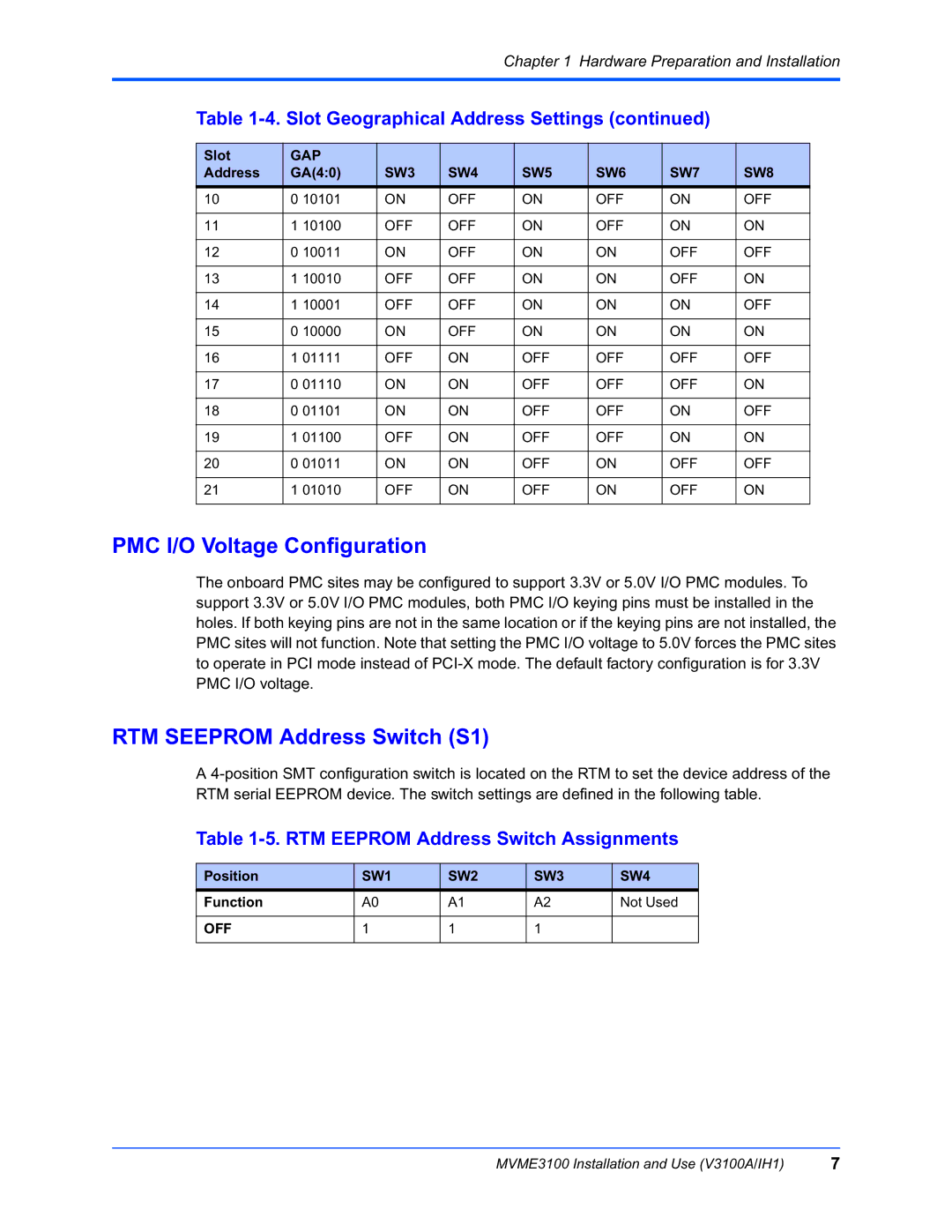
Table 1-4. Slot Geographical Address Settings (continued)
Slot | GAP |
|
|
|
|
|
|
Address | GA(4:0) | SW3 | SW4 | SW5 | SW6 | SW7 | SW8 |
10 | 0 10101 | ON | OFF | ON | OFF | ON | OFF |
|
|
|
|
|
|
|
|
11 | 1 10100 | OFF | OFF | ON | OFF | ON | ON |
|
|
|
|
|
|
|
|
12 | 0 10011 | ON | OFF | ON | ON | OFF | OFF |
|
|
|
|
|
|
|
|
13 | 1 10010 | OFF | OFF | ON | ON | OFF | ON |
|
|
|
|
|
|
|
|
14 | 1 10001 | OFF | OFF | ON | ON | ON | OFF |
|
|
|
|
|
|
|
|
15 | 0 10000 | ON | OFF | ON | ON | ON | ON |
|
|
|
|
|
|
|
|
16 | 1 01111 | OFF | ON | OFF | OFF | OFF | OFF |
|
|
|
|
|
|
|
|
17 | 0 01110 | ON | ON | OFF | OFF | OFF | ON |
|
|
|
|
|
|
|
|
18 | 0 01101 | ON | ON | OFF | OFF | ON | OFF |
|
|
|
|
|
|
|
|
19 | 1 01100 | OFF | ON | OFF | OFF | ON | ON |
|
|
|
|
|
|
|
|
20 | 0 01011 | ON | ON | OFF | ON | OFF | OFF |
|
|
|
|
|
|
|
|
21 | 1 01010 | OFF | ON | OFF | ON | OFF | ON |
|
|
|
|
|
|
|
|
PMC I/O Voltage Configuration
The onboard PMC sites may be configured to support 3.3V or 5.0V I/O PMC modules. To support 3.3V or 5.0V I/O PMC modules, both PMC I/O keying pins must be installed in the holes. If both keying pins are not in the same location or if the keying pins are not installed, the PMC sites will not function. Note that setting the PMC I/O voltage to 5.0V forces the PMC sites to operate in PCI mode instead of
RTM SEEPROM Address Switch (S1)
A
Table 1-5. RTM EEPROM Address Switch Assignments
Position | SW1 | SW2 | SW3 | SW4 |
Function | A0 | A1 | A2 | Not Used |
|
|
|
|
|
OFF | 1 | 1 | 1 |
|
|
|
|
|
|
MVME3100 Installation and Use (V3100A/IH1) | 7 |
