Chapter 4 Functional Description
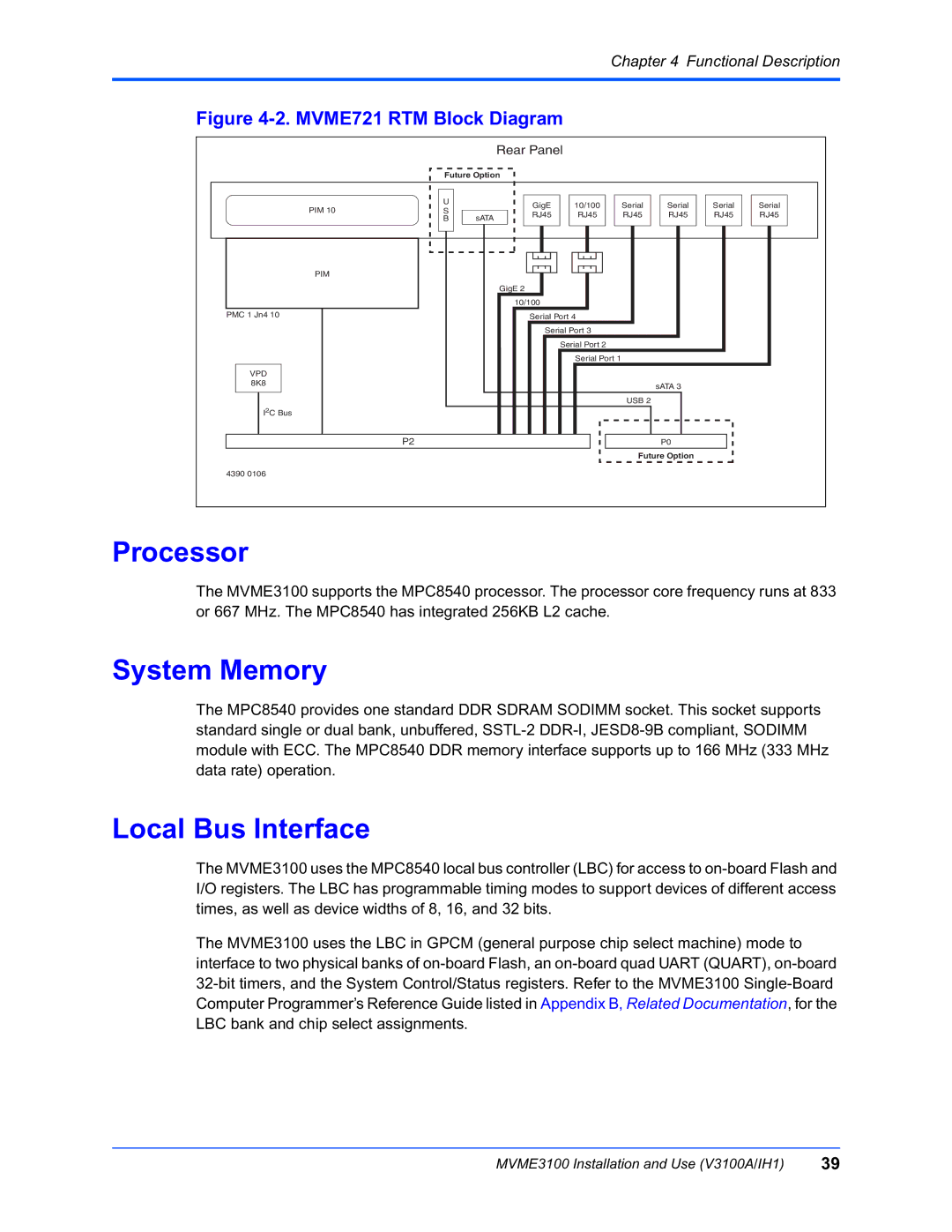
Figure 4-2. MVME721 RTM Block Diagram
Rear Panel
Future Option
PIM 10
U
S B
sATA
GigE RJ45
10/100
RJ45
Serial RJ45
Serial RJ45
Serial RJ45
Serial RJ45
PIM
PMC 1 Jn4 10
VPD
8K8
I2C Bus
GigE 2
10/100
Serial Port 4
Serial Port 3
Serial Port 2
Serial Port 1
sATA 3
USB 2
P2
P0
Future Option
4390 0106
Processor
The MVME3100 supports the MPC8540 processor. The processor core frequency runs at 833 or 667 MHz. The MPC8540 has integrated 256KB L2 cache.
System Memory
The MPC8540 provides one standard DDR SDRAM SODIMM socket. This socket supports standard single or dual bank, unbuffered,
Local Bus Interface
The MVME3100 uses the MPC8540 local bus controller (LBC) for access to
The MVME3100 uses the LBC in GPCM (general purpose chip select machine) mode to interface to two physical banks of
MVME3100 Installation and Use (V3100A/IH1) | 39 |