R61509V
R61509V
112
139
Rev .11 April 25, 2008, page 5
Description
Features
VGL
Power Supply Specifications
Difference Between R61509 and R61509V
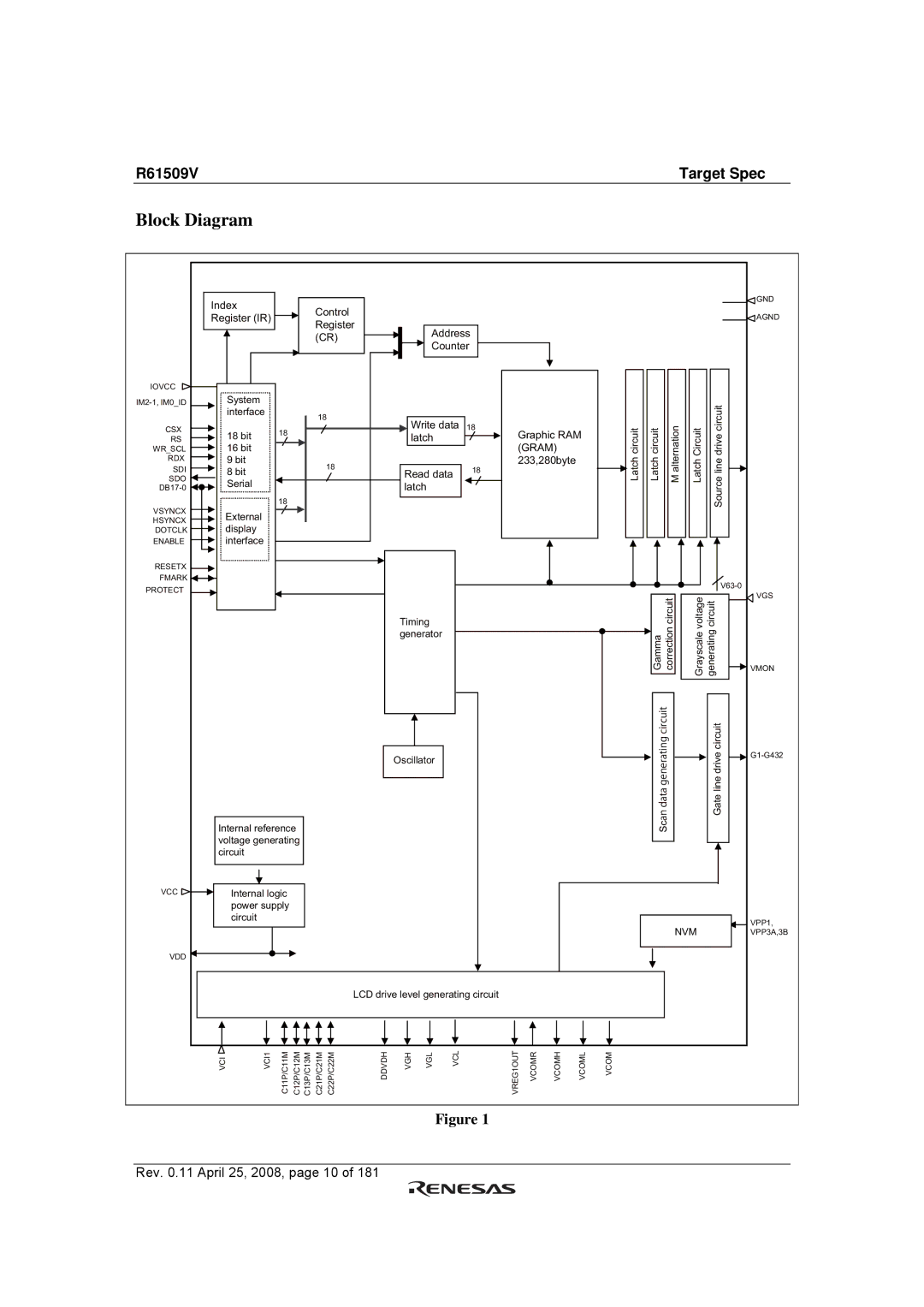
Block Diagram
Gram
System Interface
Block Function
Register Selection Clock Synchronous Serial Interface
SDI
External Display Interface RGB, Vsync interfaces
Address Counter AC
SDO
Graphics RAM Gram
Liquid Crystal Drive Power Supply Circuit
Internal Logic Power Supply Regulator
Grayscale Voltage Generating Circuit
Pin Function
External Power Supply
Bus Interface Amplitude IOVCC~GND
Vsyncx
Enable
Resetx
GND Iovcc Hsyncx
VDD
Internal Power Supply Circuit
Protect
VCI1
LCD drive
Others test, dummy pins
R61509V Pad Arrangement Rev
Alignment marks Axis
Type a 9381.0 251.0
AGNDDUM1
DUMMYR1
DUMMYR2
VPP3B
DB2
GNDDUM8
DB3
DB1
AGNDDUM5
AGNDDUM3
AGNDDUM4
TESTO1
R61509V Pad Coordinate (Unit:μm)
VGLDMY2
TESTO5
R61509V Pad Coordinate (Unit:μm)
R61509V Pad Coordinate (Unit:μm)
R61509V Pad Coordinate (Unit:μm)
TESTO8
TESTO6
TESTO7
TESTO9
R61509V Pad Coordinate (Unit:μm)
R61509V Pad Coordinate (Unit:μm)
R61509V Pad Coordinate (Unit:μm)
TESTO14
VGLDMY3
R61509V Pad Coordinate (Unit:μm)
DUMMYR3
VGLDMY4
TESTO15
DUMMYR4
Bump Arrangement
Rev .11 April 25, 2008, page 36
R61509V Wiring Example & Recommended Wiring Resistance
Gram Address Map
Gram address and display position on the panel SS = 0, BGR =
Gram address and display position on the panel SS = 1, BGR =
Outline
Instruction
Instruction Data Format
Display control Device code read R000h
Index IR
Driver Output Control R001h
Entry Mode R003h
LCD Drive Wave Control R002h
Rev .11 April 25, 2008, page 43
Automatic Address Update ORG = 0, AM, ID
Display Control 1 R007h
Display Control 2 R008h
Front and Back Porch Periods
Display Control 3 R009h
Color Control R00Bh
External Display Interface Control 1 R00Ch
RAM Access Interface
Display Interface
ENC20 Sets the RAM write cycle via RGB interface
External Display Interface Control 2 R00Fh
Clocks per Line Internal Clock Operation
Panel Interface Control 1 R010h
Division Ratio Internal Operation
Frame Frequency Calculation
Fosc
Panel Interface Control 2 R011h
㪭㪜㪨㪮㪠㪲㪉㪑㪇㪴 㪭㪜㪨㪮㪠㪲㪉㪑㪇㪴 㪭㪚㪠㩷㫃㪼㫍㪼㫃㩷 㩷 㪭㪚㪦㪤㩷㫆㫌㫋㫇㫌㫋 㪞㪥㪛㩷㫃㪼㫍㪼㫃㩷
Panel Interface Control 3 R012h
SEQWI20 Source Equalize Period
Panel Interface Control 4 R013h
Panel Interface Control 5 R014h
Panel Interface Control 6 R020h
Division Ratio of Dotclk RGB interface operation
Dotclkd in 1H period RGB interface operation
RTNE50
Panel Interface Control 7 R021h
NOWE20 Non-overlap period
Panel Interface Control 8 R022h
SEQWE20 Source Equalize Period
Panel Interface Control 9 R023h
Mcpe 20 Vcom alternating point
Frame Marker Control R090h
Power Control Power Control 1 R100h
Constant Current in Operational Amplifiers
Ddvdh VCL VGH VGL
Step-Up Factor for Step-Up Circuits
VCI1+DDVDH
Step-up Frequency Step-up Circuit
Power Control 2 R101h
Step-up clock frequency for Step-up Circuit
Line frequency
VC20 Sets VCI voltage level
DC0x Value and DCDC1 Step-up Clock Signal Waveform Example
Power Control3 R102h
VRH30 Sets the factor to generate VREG1OUT
Power Control 4 R103h
Gram Address setting range
Gram Data Write R202h
RGB
Gram Data Read R202h
Gram Read Sequence
NVM Data Read / NVM Data Write R280h
Rev .11 April 25, 2008, page 79
R61509V Target Spec
Gram Address Map and Window Address Area
Control Control 1 ~ 14 R300h to R309h
R61509V Target Spec
NDL
VLE
Rev .11 April 25, 2008, page 86
Gate scan start position SCN50 SM=0 SM=1 GS=0 GS=1
Rev .11 April 25, 2008, page 88
Pin Control Test Register Software Reset R600h
’h0 Halt ’h1 Write ’h2 Setting disabled ’h3 Erase
Rev .11 April 25, 2008, page 91
R61509V Instruction List Rev 0.50 2008
Initial state of input/output pins* see Note
Reset Function
Initial state of instruction bits default
RAM Data initialization
Rev .11 April 25, 2008, page 94
Basic Mode Operation of the R61509V
OFF
Interface and Data Format
Operation Modes
Internal clock operation
RGB interface operation
Vsync interface operation
Fmark interface operation
IM Bit Settings and System Interface
System Interface
WRX R61509V
WR R61509V
R61509V
16-bit Data Transfer Synchronization
System 9-bit Bus Interface
Bit Interface
Bit Data Transfer Synchronization
WRX R61509V
System 8-bit Bus Interface
Bit Interface Data Format RAM Data Write
Rev .11 April 25, 2008, page 108
Start Byte Format
Serial Interface
Functions of RS, R/W Bits
Serial Interface Data Format
Data Transfer in Serial Interface
Vsync Interface
Vsync Interface
240 ⋅ DisplayLines NL
Example
Write/Display Operation Timing via Vsync Interface
Internal clock operation
Fmark Interface
Fmark Interface
Internal oscillation frequency fosc Hz
FMP bit setting
Main panel
One frame period
FMP Setting Example
RAM physical line address
RGB Interface
RGB interface
Polarities of VSYNCX, HSYNCX, ENABLE, and Dotclk Signals
Pcdivl
RGB Interface Timing
16-/18-Bit RGB Interface Timing
RAM access via system interface in RGB interface operation
Moving Picture Display via RGB Interface
Bit RGB Interface
Example of 16-Bit RGB Interface and Data Format
Example of 18-Bit RGB Interface and Data Format
RGB and Internal Clock Operation Mode Switching Sequences
Functions Not Available in RGB Interface operation
Ptde Ptdp
RAM Address and Display Position on the Panel
Basee VSA, VEA
PTSA, Ptea
Screen setting
Restrictions in Setting Display Control Instruction
Base image display
Display RAM Address and Panel Display Position
Instruction Setting Example
Full screen display no partial display
Partial only
Partial Display
Automatic Address Update within a Window Address Area
Window Address Function
Scan Mode Setting
Scan direction
Color Display Mode
Color Display Mode
Frame-Frequency Adjustment Function
Example of Calculation when maximum frame frequency = 60 Hz
47 Hz
Partial Display Function
Basee =
Liquid Crystal Panel Interface Timing
Rev .11 April 25, 2008, page 141
Correction Function
Correction Function
Correction Circuit
Reference level adjustment registers
Correction Registers
Reference Level Adjustment Registers and Resistors
Interpolation Registers
Interpolation factor for V2 to
Interpolation Factor for V56 to
Grayscale Voltage Calculation Formula
(R2~R8/SUMR
Frame Memory Data and the Grayscale Voltage
Power Supply Generating Circuit
Power Supply Circuit Connection Example 1 VCI1 = Vciout
R61509V
Capacitor
Specifications of Power-supply Circuit External Elements
Internal Logic Power Supply
Schottky Diode
Voltage Setting Pattern Diagram
Rev .11 April 25, 2008, page 153
Vcomh and VREG1OUT Voltage Adjustment Sequence
Display on Sequence
NVM Control
NVM Load Register Resetting Sequence
NVM Write Sequence
NVM Write Sequence
NVM Erase Sequence
NVM Erase Sequence
Power Supply Setting Sequence
Power Supply on Sequence
Power Supply OFF Sequence
Rev .11 April 25, 2008, page 161
Instruction Setting Sequence and Refresh Sequence
Display ON/OFF Sequences and Refresh Sequence
Shutdown Mode Sequences
Rev .11 April 25, 2008, page 164
Rev .11 April 25, 2008, page 165
Color Mode Setting
Partial Display Setting
Absolute Maximum Ratings
Electrical Characteristics
DC Characteristics
Rev .11 April 25, 2008, page 169
Internal Reference Voltage Condition
Step-up Circuit Characteristics
Vclv
VREG1O
Power Supply Voltage Range
Output Voltage Range
Vcomh VREG1OUT
AC Characteristics
Clock Characteristics
Pwdl
Clock Synchronous Serial Interface Timing Characteristics
RGB Interface Timing Characteristics
Pwdh
LCD Driver Output Characteristics
Reset Timing Characteristics (IOVCC=1.65V~3.30V)
Rev .11 April 25, 2008, page 175
Test Circuits
Timing Characteristics System Bus Interface
Figure a 80-system Bus Interface
Figure C Reset Timing
Clock Synchronous Serial Interface
Vsyncx
Renesas Sales Offices
Revision Record