Advanced Version | |
400 MHz CPU, 4.0 MB |
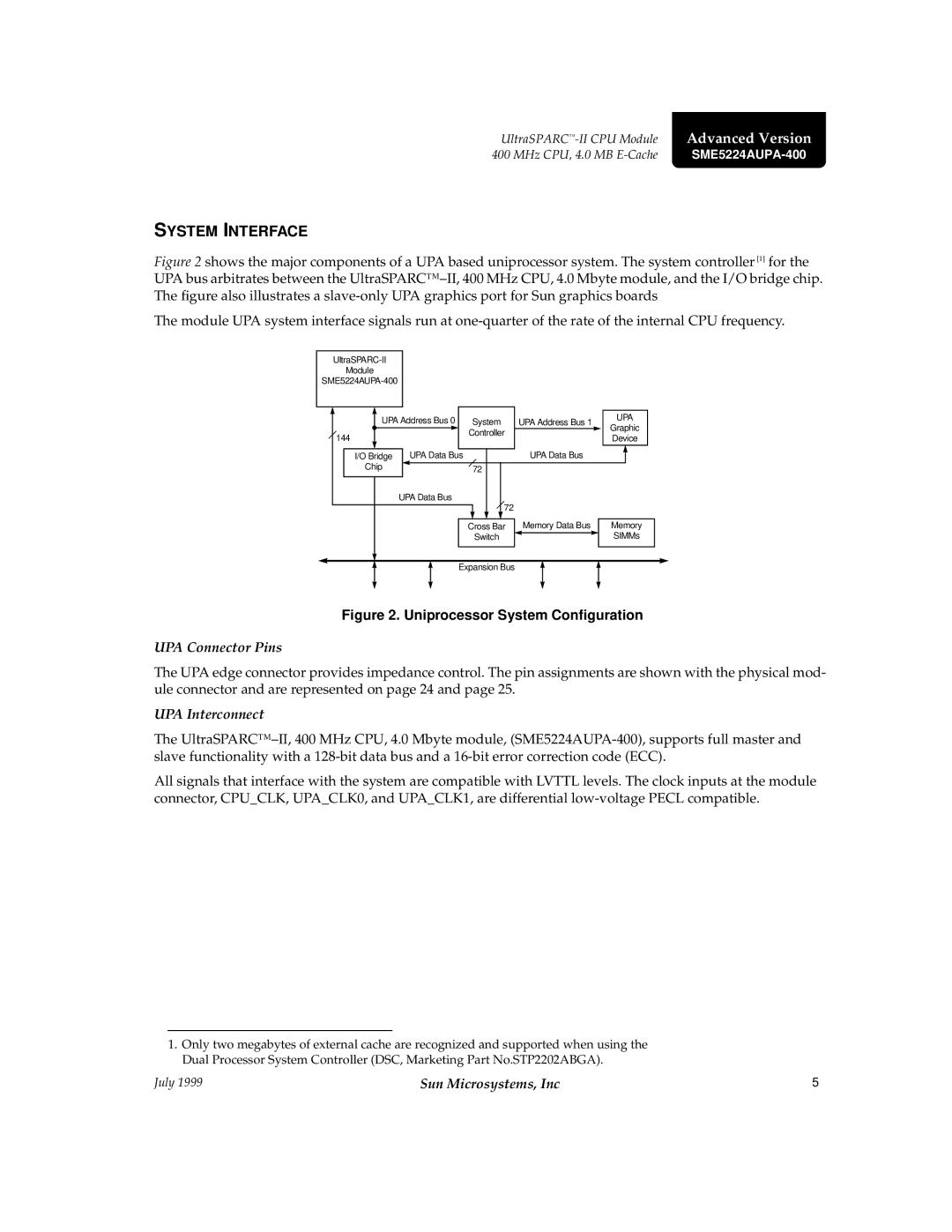
SYSTEM INTERFACE
Figure 2 shows the major components of a UPA based uniprocessor system. The system controller [1] for the UPA bus arbitrates between the UltraSPARC™–II, 400 MHz CPU, 4.0 Mbyte module, and the I/O bridge chip. The figure also illustrates a slave-only UPA graphics port for Sun graphics boards.
The module UPA system interface signals run at one-quarter of the rate of the internal CPU frequency.
|
|
|
| ||
Module |
|
|
|
| |
|
|
|
| ||
UPA Address Bus 0 | System | UPA Address Bus 1 | UPA | ||
Graphic | |||||
144 |
| Controller |
| ||
|
| Device | |||
|
|
| |||
I/O Bridge | UPA Data Bus |
| UPA Data Bus |
| |
Chip |
| 72 |
|
| |
|
|
|
| ||
| UPA Data Bus |
|
|
| |
|
| 72 |
|
| |
|
|
|
| Memory Data Bus |
| Cross Bar |
| ||
| Switch |
|
|
|
|
|
|
|
|
Memory
SIMMs
Expansion Bus
Figure 2. Uniprocessor System Configuration
UPA Connector Pins
The UPA edge connector provides impedance control. The pin assignments are shown with the physical mod- ule connector and are represented on page 24 and page 25.
UPA Interconnect
The
All signals that interface with the system are compatible with LVTTL levels. The clock inputs at the module connector, CPU_CLK, UPA_CLK0, and UPA_CLK1, are differential
1.Only two megabytes of external cache are recognized and supported when using the Dual Processor System Controller (DSC, Marketing Part No.STP2202ABGA).
July 1999 | Sun Microsystems, Inc | 5 |