Advanced Version | |
400 MHz CPU, 4.0 MB |
UPA AND CPU CLOCKS
Module Clocks
The module receives three differential pair low voltage PECL (LVPECL) clock signals (CPU_CLK, UPA_CLK0 and UPA_CLK1) from the systemboard and terminates them. The CPU_CLK is unique in the system, but the UPA_CLKs are two of many UPA clock inputs in the system.
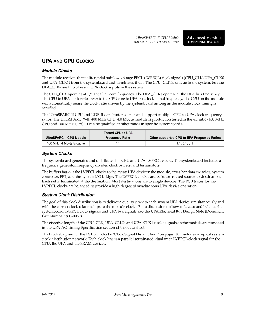
The CPU_CLK operates at 1/2 the CPU core frequency. The UPA_CLKs operate at the UPA bus frequency. The CPU to UPA clock ratios refer to the CPU core to UPA bus clock signal frequency. The CPU on the module will automatically sense the clock ratio driven by the systemboard as long as the module clock timing is satisfied.
The
| Tested CPU to UPA |
|
Frequency Ratio | Other supported CPU to UPA Frequency Ratios | |
400 MHz, 4 Mbyte | 4:1 | 3:1, 5:1, 6:1 |
|
|
|
System Clocks
The systemboard generates and distributes the CPU and UPA LVPECL clocks. The systemboard includes a frequency generator, frequency divider, clock buffers, and terminators.
The buffers
System Clock Distribution
The goal of this clock distribution is to deliver a quality clock to each system UPA device simultaneously and with the correct clock relationships to the module clocks. For a discussion on how to layout and balance the systemboard LVPECL clock signals and UPA bus signals, see the UPA Electrical Bus Design Note (Document Part Number:
The effective length of the CPU_CLK, UPA_CLK0, and UPA_CLK1 clocks signals on the module are provided in the UPA AC Timing Specification section of this data sheet.
The block diagram for the LVPECL clocks "Clock Signal Distribution," on page 10, illustrates a typical system clock distribution network. Each clock line is a
July 1999 | Sun Microsystems, Inc | 9 |
