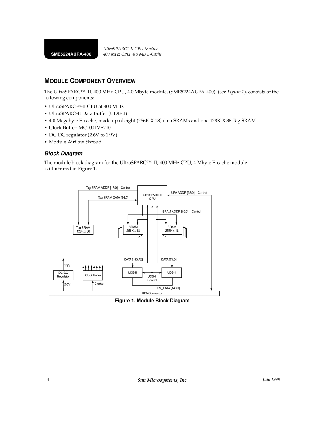
MODULE COMPONENT OVERVIEW
The
•
•
•4.0 Megabyte
•Clock Buffer: MC100LVE210
•
•Module Airflow Shroud
Block Diagram
The module block diagram for the
Tag SRAM ADDR [17:0] + Control
Tag SRAM DATA [24:0] |
CPU
UPA ADDR [35:0] + Control
Tag SRAM 128K x 36
1.9V |
| |
Clock Buffer | ||
Regulator | ||
|
| SRAM ADDR [19:0] + Control |
SRAM | SRAM |
256K x 18 | 256K x 18 |
DATA [143:72] | DATA [71:0] |
| |
| Control |
2.6V | Clocks |
UPA_DATA [143:0]
UPA Connector
Figure 1. Module Block Diagram
4 | Sun Microsystems, Inc | July 1999 |