CY7C1546V18, CY7C1557V18
CY7C1548V18, CY7C1550V18
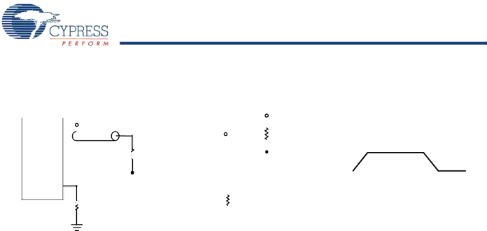
AC Test Loads and Waveforms
Figure 4. AC Test Loads and Waveforms
VREF = 0.75V
VREF |
|
|
|
|
|
|
| 0.75V |
|
| ||||
|
|
|
|
|
|
|
|
| ||||||
OUTPUT |
|
|
|
|
|
|
|
| Z0 = 50Ω |
|
| |||
|
|
|
|
|
|
|
|
|
| |||||
Device |
|
|
|
|
|
|
|
|
| |||||
Under |
|
|
|
|
|
|
|
|
|
|
|
|
| |
|
|
|
|
|
|
|
|
|
|
|
|
| ||
|
|
|
|
|
|
|
|
|
|
|
|
| ||
|
|
|
|
|
|
|
|
|
|
|
|
| ||
Test |
|
|
|
|
|
|
|
|
|
|
|
|
| |
ZQ
RQ =
![]()
![]()
![]() 250Ω
250Ω
(a)
![]()
![]() RL = 50Ω
RL = 50Ω
VREF = 0.75V
|
|
|
|
|
|
|
|
|
|
|
|
|
|
|
|
|
|
|
|
|
|
VREF |
|
|
|
|
|
| 0.75V |
|
|
|
|
| R = 50Ω | ||||||||
|
|
|
|
|
|
|
| ||||||||||||||
|
|
|
|
|
|
|
|
| |||||||||||||
OUTPUT |
|
|
|
|
|
|
|
|
|
|
|
|
|
|
|
|
| ALL INPUT PULSES[21] | |||
|
|
|
|
|
|
|
|
|
|
|
|
|
|
|
| ||||||
|
|
|
|
|
|
|
|
|
|
|
|
|
|
| 1.25V | ||||||
|
|
|
|
|
|
|
|
|
|
|
|
|
|
| |||||||
Device |
|
|
|
|
|
|
|
|
|
|
|
|
|
|
|
| 5 pF 0.25V |
|
|
| 0.75V |
|
|
|
|
|
|
|
|
|
|
|
|
|
|
|
|
|
|
| |||
|
|
|
|
|
|
|
|
|
|
|
|
|
|
|
|
|
|
|
| ||
Under | ZQ |
|
|
|
|
|
|
|
|
|
|
|
|
|
|
|
| Slew Rate = 2 V/ns | |||
|
|
|
|
|
|
|
|
|
|
|
|
|
|
| |||||||
|
|
|
|
|
|
|
|
|
|
|
|
|
|
|
| ||||||
Test |
|
|
|
|
|
| RQ = |
|
|
|
|
|
|
|
|
| |||||
|
|
|
|
|
|
|
|
|
|
| |||||||||||
|
|
|
|
|
|
|
|
|
|
|
|
|
|
| |||||||
|
|
|
|
|
|
|
|
|
|
|
|
|
|
|
|
|
|
|
| ||
|
|
|
|
|
|
|
|
|
|
|
|
|
|
|
|
| |||||
|
|
|
|
|
|
|
|
| 250Ω |
|
|
|
|
|
|
|
|
|
| ||
INCLUDING |
|
|
|
|
|
|
|
|
|
|
|
|
|
|
|
| |||||
|
|
|
|
|
|
|
|
|
|
|
|
|
|
|
| ||||||
JIG AND |
|
|
|
|
|
| (b) |
|
|
|
|
|
|
|
|
|
| ||||
|
|
|
|
|
|
|
|
|
|
|
|
|
|
|
| ||||||
|
|
|
|
|
|
|
|
|
|
|
|
|
|
|
| ||||||
SCOPE |
|
|
|
|
|
|
|
|
|
|
|
|
|
|
|
| |||||
Note
21.Unless otherwise noted, test conditions assume signal transition time of 2V/ns, timing reference levels of 0.75V, VREF = 0.75V, RQ = 250Ω, VDDQ = 1.5V, input pulse levels of 0.25V to 1.25V, output loading of the specified IOL/IOH, and load capacitance shown in (a) of AC Test Loads and Waveforms.
Document Number: | Page 22 of 28 |
[+] Feedback