| bdiGDB for GNU Debugger, BDI2000 | User Manual | 7 | |||||
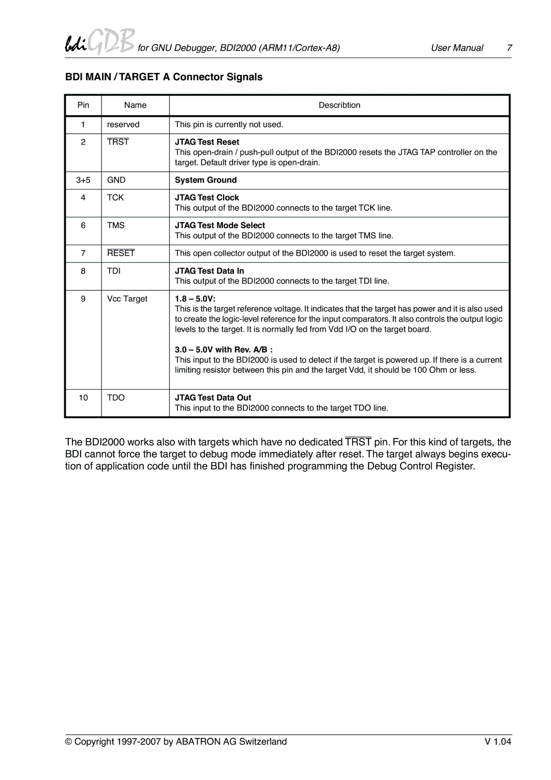
| BDI MAIN / TARGET A Connector Signals |
|
| |||||
|
|
|
|
|
|
| ||
| Pin |
| Name | Describtion |
|
| ||
|
|
|
|
|
|
| ||
| 1 |
| reserved | This pin is currently not used. |
|
| ||
|
|
|
|
|
|
|
|
|
| 2 |
|
|
|
| JTAG Test Reset |
|
|
| TRST |
|
| |||||
|
|
|
|
|
| This |
| |
|
|
|
|
|
| target. Default driver type is |
|
|
|
|
|
|
|
|
| ||
| 3+5 |
| GND | System Ground |
|
| ||
|
|
|
|
|
|
| ||
| 4 |
| TCK | JTAG Test Clock |
|
| ||
|
|
|
|
|
| This output of the BDI2000 connects to the target TCK line. |
|
|
|
|
|
|
|
|
| ||
| 6 |
| TMS | JTAG Test Mode Select |
|
| ||
|
|
|
|
|
| This output of the BDI2000 connects to the target TMS line. |
|
|
|
|
|
|
|
|
| ||
| 7 |
|
|
|
| This open collector output of the BDI2000 is used to reset the target system. |
| |
| RESET |
| ||||||
|
|
|
|
|
|
| ||
| 8 |
| TDI | JTAG Test Data In |
|
| ||
|
|
|
|
|
| This output of the BDI2000 connects to the target TDI line. |
|
|
|
|
|
|
|
|
| ||
| 9 |
| Vcc Target | 1.8 – 5.0V: |
|
| ||
|
|
|
|
|
| This is the target reference voltage. It indicates that the target has power and it is also used |
| |
|
|
|
|
|
| to create the |
| |
|
|
|
|
|
| levels to the target. It is normally fed from Vdd I/O on the target board. |
| |
|
|
|
|
|
| 3.0 – 5.0V with Rev. A/B : |
|
|
|
|
|
|
|
| This input to the BDI2000 is used to detect if the target is powered up. If there is a current |
| |
|
|
|
|
|
| limiting resistor between this pin and the target Vdd, it should be 100 Ohm or less. |
| |
|
|
|
|
|
|
| ||
| 10 |
| TDO | JTAG Test Data Out |
|
| ||
|
|
|
|
|
| This input to the BDI2000 connects to the target TDO line. |
|
|
|
|
|
|
|
|
|
|
|
The BDI2000 works also with targets which have no dedicated TRST pin. For this kind of targets, the BDI cannot force the target to debug mode immediately after reset. The target always begins execu- tion of application code until the BDI has finished programming the Debug Control Register.
© Copyright | V 1.04 |