|
|
|
|
| PRELIMINARY |
|
|
| CY14B101P | |
|
|
|
|
|
|
|
|
|
| |
|
|
|
|
|
|
|
|
| ||
AutoStore or Power Up RECALL |
|
|
|
|
| |||||
|
|
|
|
|
|
|
|
|
|
|
Parameters |
|
|
|
| Description |
| CY14B101P |
| Unit | |
|
|
|
| Min |
| Max |
| |||
|
|
|
|
|
|
|
|
| ||
tFA [8] |
| Power Up RECALL Duration |
|
| 20 |
| ms | |||
tSTORE [9] |
| STORE Cycle Duration |
|
| 8 |
| ms | |||
tDELAY [10] |
| Time Allowed to Complete SRAM Cycle |
|
| 25 |
| ns | |||
VSWITCH |
| Low Voltage Trigger Level |
|
| 2.65 |
| V | |||
tVCCRISE |
| VCC Rise Time | 150 |
|
|
| µs | |||
VHDIS[6] |
| HSB | Output Driver Disable Voltage |
|
| 1.9 |
| V | ||
tLZHSB |
| HSB | To Output Active Time |
|
| 5 |
| µs | ||
tHHHD |
| HSB | High Active Time |
|
| 500 |
| ns | ||
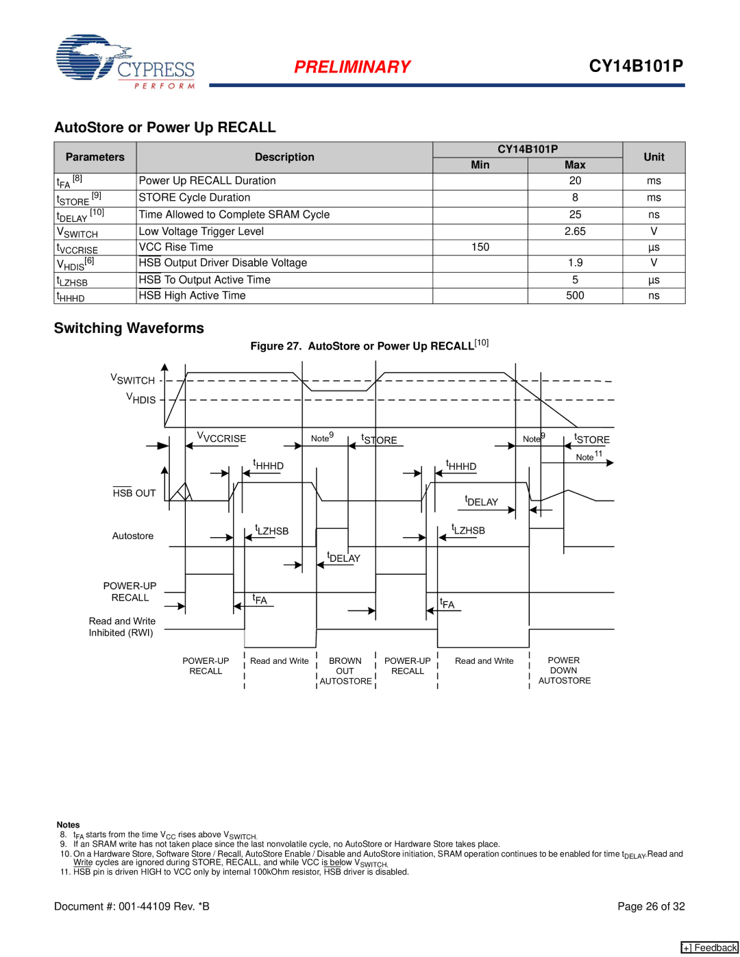
Switching Waveforms
Figure 27. AutoStore or Power Up RECALL[10]
VSWITCH
VHDIS
HSB OUT
Autostore
RECALL
Read and Write Inhibited (RWI)
VVCCRISE |
| Note9 | tSTORE | Note9 | tSTORE | |
| tHHHD |
|
|
| tHHHD | Note11 |
|
|
|
|
| ||
|
|
|
|
| tDELAY |
|
| tLZHSB |
|
|
| tLZHSB |
|
|
| tDELAY |
|
|
|
|
| tFA |
|
|
| tFA |
|
Read and Write | BROWN | Read and Write | POWER | |||
RECALL |
| OUT |
| RECALL |
| DOWN |
|
| AUTOSTORE |
| AUTOSTORE | ||
Notes
8.tFA starts from the time VCC rises above VSWITCH.
9.If an SRAM write has not taken place since the last nonvolatile cycle, no AutoStore or Hardware Store takes place.
10.On a Hardware Store, Software Store / Recall, AutoStore Enable / Disable and AutoStore initiation, SRAM operation continues to be enabled for time tDELAY.Read and Write cycles are ignored during STORE, RECALL, and while VCC is below VSWITCH.
11.HSB pin is driven HIGH to VCC only by internal 100kOhm resistor, HSB driver is disabled.
Document #: | Page 26 of 32 |
[+] Feedback