|
|
|
|
|
| PRELIMINARY |
|
|
|
| CY14B101P | ||||||
|
|
|
|
|
|
|
|
|
|
|
|
|
|
|
|
|
|
|
|
|
|
|
|
|
|
|
|
|
|
|
|
|
|
| |
Table 10. Register Map Detail (continued) |
|
|
|
|
|
|
|
|
|
|
|
| |||||
|
|
|
|
|
|
|
|
|
|
|
|
|
|
|
|
| |
|
|
|
|
|
|
|
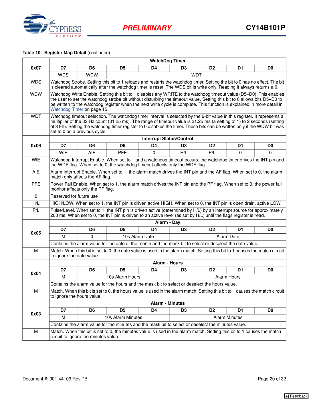
| WatchDog Timer |
|
|
|
|
|
|
| ||
0x07 |
|
|
|
|
|
|
|
|
|
|
|
|
|
|
|
| |
D7 |
|
| D6 |
| D5 |
| D4 |
| D3 |
| D2 |
| D1 |
| D0 | ||
|
|
|
|
|
|
|
|
|
|
|
|
|
|
|
| ||
| WDS | WDW |
|
|
|
|
|
| WDT |
|
|
|
|
| |||
|
|
|
|
|
|
|
|
| |||||||||
WDS | Watchdog Strobe. Setting this bit to 1 reloads and restarts the watchdog timer. Setting the bit to 0 has no effect. The bit | ||||||||||||||||
| is cleared automatically after the watchdog timer is reset. The WDS bit is write only. Reading it always returns a 0. | ||||||||||||||||
WDW | Watchdog Write Enable. Setting this bit to 1 disables any WRITE to the watchdog timeout value | ||||||||||||||||
| the user to set the watchdog strobe bit without disturbing the timeout value. Setting this bit to 0 allows bits | ||||||||||||||||
| be written to the watchdog register when the next write cycle is complete. This function is explained in more detail in | ||||||||||||||||
| Watchdog Timer on page 15. |
|
|
|
|
|
|
|
|
|
|
|
| ||||
WDT | Watchdog timeout selection. The watchdog timer interval is selected by the | ||||||||||||||||
| multiplier of the 32 Hz count (31.25 ms). The range of timeout value is 31.25 ms (a setting of 1) to 2 seconds (setting | ||||||||||||||||
| of 3 Fh). Setting the watchdog timer register to 0 disables the timer. These bits can be written only if the WDW bit was | ||||||||||||||||
| set to 0 on a previous cycle. |
|
|
|
|
|
|
|
|
|
|
|
| ||||
|
|
|
|
|
|
|
| Interrupt Status/Control |
|
|
|
|
| ||||
0x06 | D7 |
|
| D6 |
| D5 |
| D4 |
| D3 |
| D2 |
| D1 |
| D0 | |
|
|
|
|
|
|
|
|
|
|
|
|
|
|
|
|
|
|
| WIE |
|
| AIE |
| PFE |
| 0 |
| H/L |
| P/L |
| 0 |
| 0 |
|
|
|
|
|
|
|
|
|
| |||||||||
WIE | Watchdog Interrupt Enable. When set to 1 and a watchdog timeout occurs, the watchdog timer drives the INT pin and | ||||||||||||||||
| the WDF flag. When set to 0, the watchdog timeout affects only the WDF flag. |
|
|
|
|
| |||||||||||
AIE | Alarm Interrupt Enable. When set to 1, the alarm match drives the INT pin and the AF flag. When set to 0, the alarm | ||||||||||||||||
| match only affects the AF flag. |
|
|
|
|
|
|
|
|
|
|
|
| ||||
PFE | Power Fail Enable. When set to 1, the alarm match drives the INT pin and the PF flag. When set to 0, the power fail | ||||||||||||||||
| monitor affects only the PF flag. |
|
|
|
|
|
|
|
|
|
|
|
| ||||
0 | Reserved for future use |
|
|
|
|
|
|
|
|
|
|
|
| ||||
|
| ||||||||||||||||
H/L | HIGH/LOW. When set to 1, the INT pin is driven active HIGH. When set to 0, the INT pin is open drain, active LOW. | ||||||||||||||||
|
| ||||||||||||||||
P/L | Pulse/Level. When set to 1, the INT pin is driven active (determined by H/L) by an interrupt source for approximately | ||||||||||||||||
| 200 ms. When set to 0, the INT pin is driven to an active level (as set by H/L) until the flags register is read. |
|
| ||||||||||||||
|
|
|
|
|
|
|
| Alarm - Day |
|
|
|
|
|
|
| ||
|
|
|
|
|
|
|
|
|
|
|
|
|
|
|
|
| |
0x05 | D7 |
|
| D6 |
| D5 |
| D4 |
| D3 |
| D2 |
| D1 |
| D0 | |
M | 0 |
| 10s Alarm Date |
|
|
|
| Alarm Date |
|
| |||||||
|
|
|
|
|
|
|
| ||||||||||
|
|
|
|
|
|
| |||||||||||
| Contains the | alarm value for | the date of the month and the | mask bit to select or deselect the date value. |
|
| |||||||||||
|
| ||||||||||||||||
M | Match. When this bit is set to 0, the date value is used in the alarm match. Setting this bit to 1 causes the match circuit | ||||||||||||||||
| to ignore the date value. |
|
|
|
|
|
|
|
|
|
|
|
| ||||
|
|
|
|
|
|
|
| Alarm - Hours |
|
|
|
|
|
|
| ||
0x04 | D7 |
|
| D6 |
| D5 |
| D4 |
| D3 |
| D2 |
| D1 |
| D0 | |
|
|
|
|
|
|
|
|
|
|
|
|
|
|
|
|
| |
M |
|
| 10s Alarm Hours |
|
|
|
| Alarm Hours |
|
| |||||||
|
|
|
|
|
|
|
|
| |||||||||
|
|
|
|
|
| ||||||||||||
| Contains the | alarm value for the hours and the mask bit to | select or deselect the hours value. |
|
| ||||||||||||
|
| ||||||||||||||||
M | Match. When this bit is set to 0, the hours value is used in the alarm match. Setting this bit to 1 causes the match circuit | ||||||||||||||||
| to ignore the hours value. |
|
|
|
|
|
|
|
|
|
|
|
| ||||
|
|
|
|
|
|
|
| Alarm - Minutes |
|
|
|
|
|
|
| ||
|
|
|
|
|
|
|
|
|
|
|
|
|
|
|
|
| |
0x03 | D7 |
|
| D6 |
| D5 |
| D4 |
| D3 |
| D2 |
| D1 |
| D0 | |
|
|
|
|
|
|
|
|
|
|
|
|
|
|
|
|
| |
M |
|
| 10s Alarm Minutes |
|
|
|
| Alarm Minutes |
|
| |||||||
|
|
|
|
|
|
|
|
| |||||||||
|
|
|
|
|
|
|
|
| |||||||||
| Contains the | alarm value for the minutes and the mask bit to select or deselect the minutes value. |
|
| |||||||||||||
|
| ||||||||||||||||
M | Match. When this bit is set to 0, the minutes value is used in the alarm match. Setting this bit to 1 causes the match | ||||||||||||||||
| circuit to ignore the minutes value. |
|
|
|
|
|
|
|
|
|
| ||||||
Document #: | Page 20 of 32 |
[+] Feedback