|
|
|
|
|
| PRELIMINARY |
|
|
|
| CY14B101P | ||||
|
|
|
|
|
|
|
|
|
|
|
|
|
|
| |
|
|
|
|
|
|
|
|
|
|
|
|
|
| ||
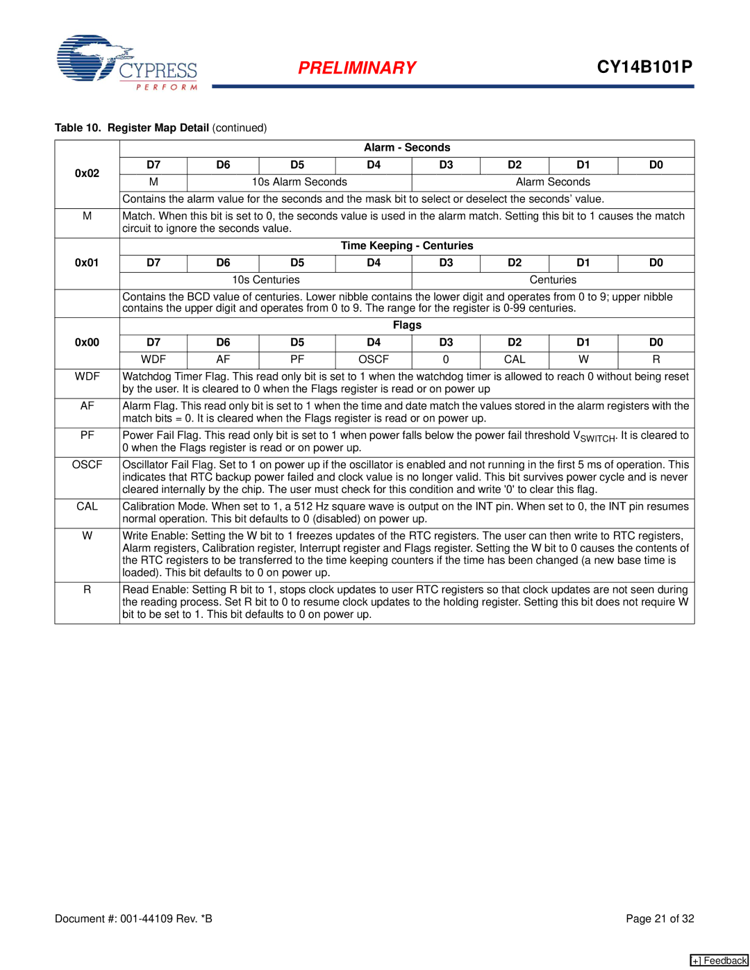
Table 10. Register Map Detail (continued) |
|
|
|
|
|
|
|
|
| ||||||
|
|
|
|
|
|
|
|
|
|
|
|
|
|
| |
|
|
|
|
|
|
| Alarm - Seconds |
|
|
|
|
| |||
|
|
|
|
|
|
|
|
|
|
|
|
|
|
| |
0x02 | D7 |
|
| D6 |
| D5 | D4 |
| D3 |
| D2 |
| D1 | D0 | |
|
|
|
|
|
|
|
|
|
|
|
|
|
|
| |
M |
|
|
| 10s Alarm Seconds |
|
|
| Alarm Seconds |
|
| |||||
|
|
|
|
|
|
|
|
| |||||||
|
|
|
|
|
|
|
| ||||||||
| Contains the | alarm value for the seconds and the mask bit to select or deselect the seconds’ value. |
|
| |||||||||||
|
| ||||||||||||||
M | Match. When this bit is set to 0, the seconds value is used in the alarm match. Setting this bit to 1 causes the match | ||||||||||||||
| circuit to ignore the seconds value. |
|
|
|
|
|
|
|
|
| |||||
|
|
|
|
|
|
| Time Keeping - Centuries |
|
|
|
|
| |||
0x01 |
|
|
|
|
|
|
|
|
|
|
|
|
|
| |
D7 |
|
| D6 |
| D5 | D4 |
| D3 |
| D2 |
| D1 | D0 | ||
|
|
|
|
| 10s | Centuries |
|
|
|
|
| Centuries |
|
| |
|
|
| |||||||||||||
| Contains the BCD value of centuries. Lower nibble contains | the lower digit and operates from 0 to 9; upper nibble | |||||||||||||
| contains the upper digit and operates from 0 to 9. The range for the register is |
|
| ||||||||||||
|
|
|
|
|
|
| Flags |
|
|
|
|
|
|
| |
0x00 | D7 |
|
| D6 |
| D5 | D4 |
| D3 |
| D2 |
| D1 | D0 | |
|
|
|
|
|
|
|
|
|
|
|
|
|
|
| |
| WDF |
|
| AF |
| PF | OSCF |
| 0 |
| CAL |
| W | R | |
|
|
|
|
|
|
|
|
| |||||||
WDF | Watchdog Timer Flag. This read only bit is set to 1 when the watchdog timer is allowed to reach 0 without being reset | ||||||||||||||
| by the user. It is cleared to 0 when the Flags register is read or on power up |
|
|
|
|
| |||||||||
AF | Alarm Flag. This read only bit is set to 1 when the time and date match the values stored in the alarm registers with the | ||||||||||||||
| match bits = 0. It is cleared when the Flags register is read or on power up. |
|
|
|
|
| |||||||||
PF | Power Fail Flag. This read only bit is set to 1 when power falls below the power fail threshold VSWITCH. It is cleared to | ||||||||||||||
| 0 when the Flags register is read or on power up. |
|
|
|
|
|
|
| |||||||
OSCF | Oscillator Fail Flag. Set to 1 on power up if the oscillator is enabled and not running in the first 5 ms of operation. This | ||||||||||||||
| indicates that RTC backup power failed and clock value is no longer valid. This bit survives power cycle and is never | ||||||||||||||
| cleared internally by the chip. The user must check for this condition and write '0' to clear this flag. |
|
| ||||||||||||
CAL | Calibration Mode. When set to 1, a 512 Hz square wave is output on the INT pin. When set to 0, the INT pin resumes | ||||||||||||||
| normal operation. This bit defaults to 0 (disabled) on power up. |
|
|
|
|
|
|
| |||||||
W | Write Enable: Setting the W bit to 1 freezes updates of the RTC registers. The user can then write to RTC registers, | ||||||||||||||
| Alarm registers, Calibration register, Interrupt register and Flags register. Setting the W bit to 0 causes the contents of | ||||||||||||||
| the RTC registers to be transferred to the time keeping counters if the time has been changed (a new base time is | ||||||||||||||
| loaded). This bit defaults to 0 on power up. |
|
|
|
|
|
|
|
|
| |||||
R | Read Enable: Setting R bit to 1, stops clock updates to user RTC registers so that clock updates are not seen during | ||||||||||||||
| the reading process. Set R bit to 0 to resume clock updates to the holding register. Setting this bit does not require W | ||||||||||||||
| bit to be set to 1. This bit defaults to 0 on power up. |
|
|
|
|
|
|
| |||||||
Document #: | Page 21 of 32 |
[+] Feedback