|
| PRELIMINARY | CY14B101P | |
|
|
|
| |
|
| cycle is in progress. The RECALL operation in no way alters the | ||
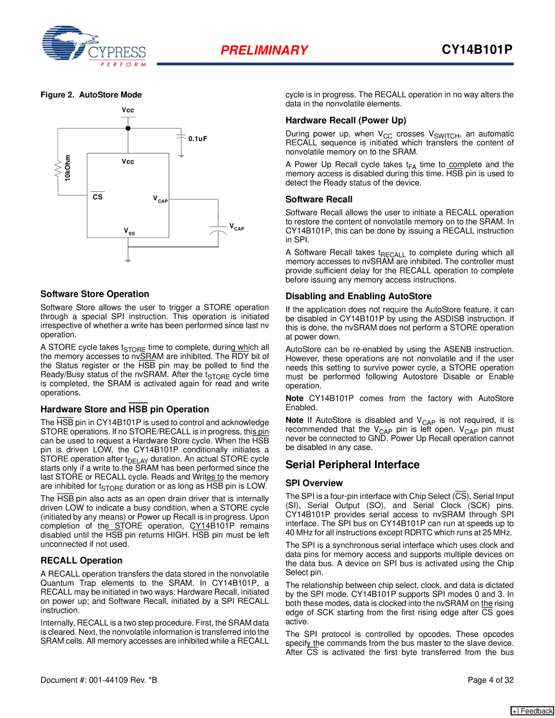
Figure 2. AutoStore Mode |
| |||
Vcc |
| data in the nonvolatile elements. |
|
|
|
|
|
| |
![]() 10kOhm
10kOhm
![]() 0.1uF
0.1uF
Vcc
CSVCAP
VSS
Hardware Recall (Power Up)
During power up, when VCC crosses VSWITCH, an automatic RECALL sequence is initiated which transfers the content of nonvolatile memory on to the SRAM.
A Power Up Recall cycle takes tFA time to complete and the memory access is disabled during this time. HSB pin is used to detect the Ready status of the device.
Software Recall
Software Recall allows the user to initiate a RECALL operation
Vto restore the content of nonvolatile memory on to the SRAM. In
CAPCY14B101P, this can be done by issuing a RECALL instruction
in SPI.
A Software Recall takes tRECALL to complete during which all memory accesses to nvSRAM are inhibited. The controller must provide sufficient delay for the RECALL operation to complete before issuing any memory access instructions.
Software Store Operation
Software Store allows the user to trigger a STORE operation through a special SPI instruction. This operation is initiated irrespective of whether a write has been performed since last nv operation.
A STORE cycle takes tSTORE time to complete, during which all the memory accesses to nvSRAM are inhibited. The RDY bit of the Status register or the HSB pin may be polled to find the Ready/Busy status of the nvSRAM. After the tSTORE cycle time is completed, the SRAM is activated again for read and write operations.
Hardware Store and HSB pin Operation
The HSB pin in CY14B101P is used to control and acknowledge STORE operations. If no STORE/RECALL is in progress, this pin can be used to request a Hardware Store cycle. When the HSB pin is driven LOW, the CY14B101P conditionally initiates a STORE operation after tDELAY duration. An actual STORE cycle starts only if a write to the SRAM has been performed since the last STORE or RECALL cycle. Reads and Writes to the memory are inhibited for tSTORE duration or as long as HSB pin is LOW.
The HSB pin also acts as an open drain driver that is internally driven LOW to indicate a busy condition, when a STORE cycle (initiated by any means) or Power up Recall is in progress. Upon completion of the STORE operation, CY14B101P remains disabled until the HSB pin returns HIGH. HSB pin must be left unconnected if not used.
RECALL Operation
A RECALL operation transfers the data stored in the nonvolatile Quantum Trap elements to the SRAM. In CY14B101P, a RECALL may be initiated in two ways: Hardware Recall, initiated on power up; and Software Recall, initiated by a SPI RECALL instruction.
Internally, RECALL is a two step procedure. First, the SRAM data is cleared. Next, the nonvolatile information is transferred into the SRAM cells. All memory accesses are inhibited while a RECALL
Disabling and Enabling AutoStore
If the application does not require the AutoStore feature, it can be disabled in CY14B101P by using the ASDISB instruction. If this is done, the nvSRAM does not perform a STORE operation at power down.
AutoStore can be
Note CY14B101P comes from the factory with AutoStore Enabled.
Note If AutoStore is disabled and VCAP is not required, it is recommended that the VCAP pin is left open. VCAP pin must never be connected to GND. Power Up Recall operation cannot be disabled in any case.
Serial Peripheral Interface
SPI Overview
The SPI is a
The SPI is a synchronous serial interface which uses clock and data pins for memory access and supports multiple devices on the data bus. A device on SPI bus is activated using the Chip Select pin.
The relationship between chip select, clock, and data is dictated by the SPI mode. CY14B101P supports SPI modes 0 and 3. In both these modes, data is clocked into the nvSRAM on the rising edge of SCK starting from the first rising edge after CS goes active.
The SPI protocol is controlled by opcodes. These opcodes specify the commands from the bus master to the slave device. After CS is activated the first byte transferred from the bus
Document #: | Page 4 of 32 |
[+] Feedback