CY7C1440AV33
CY7C1442AV33
CY7C1446AV33
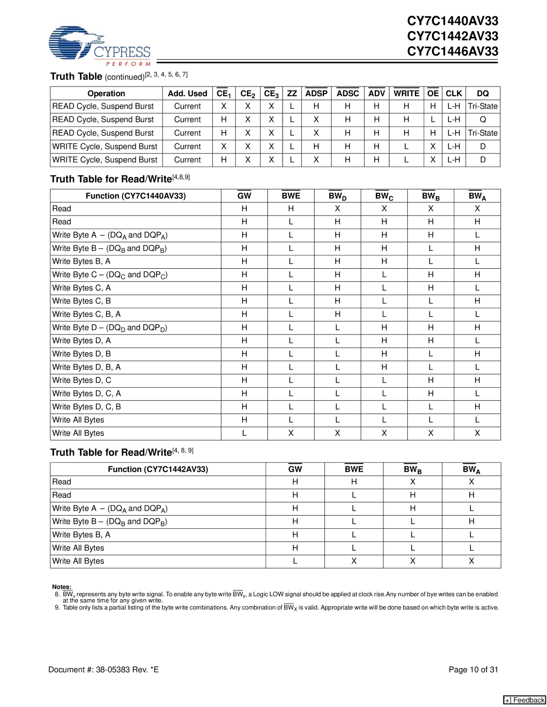
Truth Table (continued)[2, 3, 4, 5, 6, 7]
Operation | Add. Used | CE1 | CE2 | CE3 | ZZ | ADSP | ADSC | ADV | WRITE | OE | CLK | DQ |
READ Cycle, Suspend Burst | Current | X | X | X | L | H | H | H | H | H | ||
|
|
|
|
|
|
|
|
|
|
|
|
|
READ Cycle, Suspend Burst | Current | H | X | X | L | X | H | H | H | L | Q | |
|
|
|
|
|
|
|
|
|
|
|
|
|
READ Cycle, Suspend Burst | Current | H | X | X | L | X | H | H | H | H | ||
|
|
|
|
|
|
|
|
|
|
|
|
|
WRITE Cycle, Suspend Burst | Current | X | X | X | L | H | H | H | L | X | D | |
|
|
|
|
|
|
|
|
|
|
|
|
|
WRITE Cycle, Suspend Burst | Current | H | X | X | L | X | H | H | L | X | D | |
|
|
|
|
|
|
|
|
|
|
|
|
|
Truth Table for Read/Write[4,8,9]
Function (CY7C1440AV33) | GW | BWE | BWD | BWC | BWB | BWA |
Read | H | H | X | X | X | X |
|
|
|
|
|
|
|
Read | H | L | H | H | H | H |
|
|
|
|
|
|
|
Write Byte A – (DQA and DQPA) | H | L | H | H | H | L |
Write Byte B – (DQB and DQPB) | H | L | H | H | L | H |
Write Bytes B, A | H | L | H | H | L | L |
|
|
|
|
|
|
|
Write Byte C – (DQC and DQPC) | H | L | H | L | H | H |
Write Bytes C, A | H | L | H | L | H | L |
|
|
|
|
|
|
|
Write Bytes C, B | H | L | H | L | L | H |
|
|
|
|
|
|
|
Write Bytes C, B, A | H | L | H | L | L | L |
|
|
|
|
|
|
|
Write Byte D – (DQD and DQPD) | H | L | L | H | H | H |
Write Bytes D, A | H | L | L | H | H | L |
|
|
|
|
|
|
|
Write Bytes D, B | H | L | L | H | L | H |
|
|
|
|
|
|
|
Write Bytes D, B, A | H | L | L | H | L | L |
|
|
|
|
|
|
|
Write Bytes D, C | H | L | L | L | H | H |
|
|
|
|
|
|
|
Write Bytes D, C, A | H | L | L | L | H | L |
|
|
|
|
|
|
|
Write Bytes D, C, B | H | L | L | L | L | H |
|
|
|
|
|
|
|
Write All Bytes | H | L | L | L | L | L |
|
|
|
|
|
|
|
Write All Bytes | L | X | X | X | X | X |
|
|
|
|
|
|
|
Truth Table for Read/Write[4, 8, 9]
Function (CY7C1442AV33) | GW | BWE | BWB | BWA |
Read | H | H | X | X |
|
|
|
|
|
Read | H | L | H | H |
|
|
|
|
|
Write Byte A – (DQA and DQPA) | H | L | H | L |
Write Byte B – (DQB and DQPB) | H | L | L | H |
Write Bytes B, A | H | L | L | L |
|
|
|
|
|
Write All Bytes | H | L | L | L |
|
|
|
|
|
Write All Bytes | L | X | X | X |
|
|
|
|
|
Notes:
8.BWx represents any byte write signal. To enable any byte write BWx, a Logic LOW signal should be applied at clock rise.Any number of bye writes can be enabled at the same time for any given write.
9.Table only lists a partial listing of the byte write combinations. Any combination of BWX is valid. Appropriate write will be done based on which byte write is active.
Document #: | Page 10 of 31 |
[+] Feedback