CY7C1440AV33
CY7C1442AV33
CY7C1446AV33
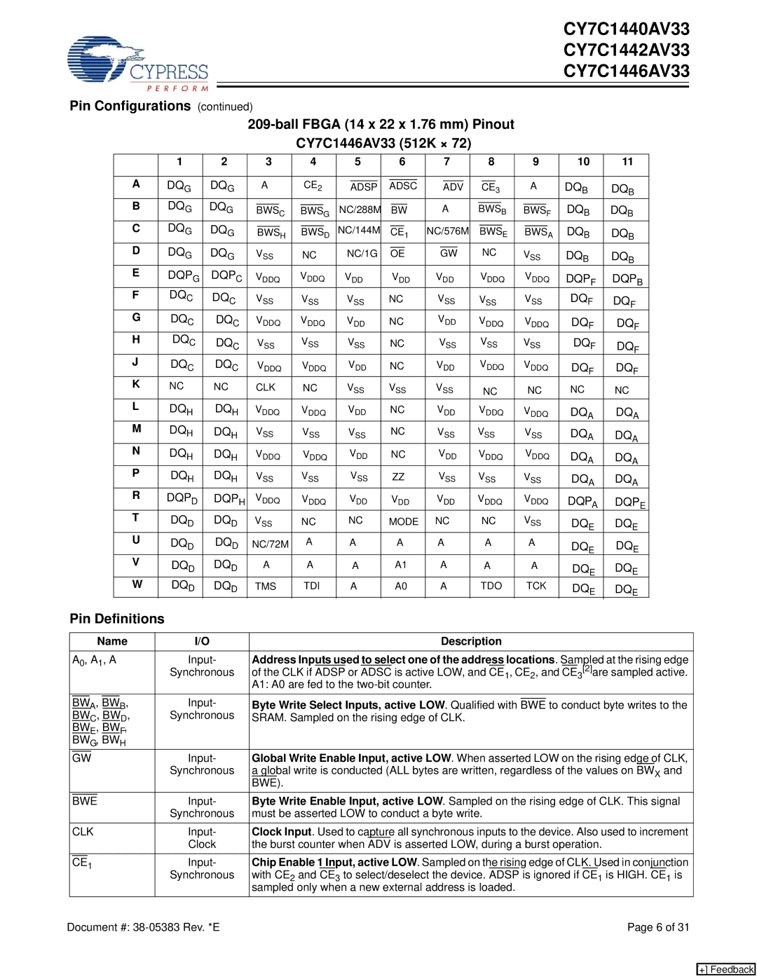
Pin Configurations (continued)
| 1 | 2 |
|
|
|
| 3 |
|
|
| 4 |
| 5 |
|
|
|
|
|
| 6 |
|
|
|
| 7 |
|
|
|
|
| 8 |
|
|
|
|
|
| 9 |
|
| 10 | 11 |
|
| ||||||
|
|
|
|
|
|
|
|
|
|
|
|
|
|
|
|
|
|
|
|
|
|
|
|
|
|
|
|
|
|
|
|
|
|
|
|
|
|
|
| |||||||||||
A | DQG | DQG |
|
| A |
|
| CE2 |
|
|
|
|
|
|
|
|
|
|
|
|
|
|
|
|
|
|
|
|
|
| A |
|
| DQB |
|
| ||||||||||||||
|
|
|
|
|
| ADSP |
|
|
| ADSC |
|
| ADV |
|
|
| CE | 3 |
|
|
|
|
| DQB |
| |||||||||||||||||||||||||
B | DQG | DQG |
|
|
|
|
|
|
|
|
|
|
|
|
|
|
|
|
| A |
|
|
|
|
|
|
|
|
|
| DQ |
|
| DQ |
|
|
| |||||||||||||
|
|
|
|
|
|
| NC/288M |
|
|
|
|
|
|
|
| BWS |
|
|
|
|
|
|
|
|
|
| ||||||||||||||||||||||||
| BWS | C |
| BWS | G |
| BW |
|
| B |
| BWS | F | B |
|
|
| |||||||||||||||||||||||||||||||||
|
|
|
|
|
|
|
|
|
|
|
|
|
|
|
|
|
|
|
|
|
|
|
|
|
|
|
|
|
|
|
|
|
|
|
|
|
|
|
|
| B |
|
| |||||||
C | DQG | DQG |
|
|
|
|
|
|
| NC/144M |
|
|
|
|
|
|
|
| NC/576M |
|
|
|
|
|
|
|
|
| DQ |
|
|
|
|
|
| |||||||||||||||
|
| BWS | H |
| BWS | D |
|
|
| CE | 1 |
|
| BWS | E |
|
| BWS | A | B | DQB |
| ||||||||||||||||||||||||||||
|
|
|
|
|
|
|
|
|
|
|
|
|
|
|
|
|
|
|
|
|
|
|
|
|
|
|
|
|
|
|
|
|
|
|
|
|
|
|
| |||||||||||
D | DQG | DQG |
| VSS |
|
|
|
| NC/1G |
|
|
|
|
|
|
|
|
|
|
|
|
| NC |
|
|
|
|
|
|
|
|
|
|
|
|
| ||||||||||||||
|
|
| NC |
|
|
|
| OE |
|
|
|
| GW |
| VSS |
|
| DQ |
|
| DQ | B |
| |||||||||||||||||||||||||||
|
|
|
|
|
|
|
|
|
|
|
|
|
|
|
|
|
|
|
|
|
|
|
|
|
|
|
|
|
|
|
|
|
|
|
|
|
|
|
|
|
|
|
| B |
|
| ||||
E | DQPG | DQPC | VDDQ | VDDQ | VDD |
|
|
|
| VDD | VDD |
| VDDQ |
|
| VDDQ | DQP | DQP |
| |||||||||||||||||||||||||||||||
|
|
|
|
|
|
|
|
|
|
|
|
|
|
|
|
|
|
|
|
|
|
|
|
|
|
|
|
|
|
|
|
|
|
|
|
|
|
|
|
|
|
|
|
|
| F |
|
| B | |
F | DQC | DQC |
| VSS |
|
| VSS |
| VSS |
| NC |
|
|
| VSS |
| VSS |
|
| VSS |
|
| DQF | DQF |
| |||||||||||||||||||||||||
G | DQC | DQC | VDDQ |
| VDDQ | VDD |
|
| NC |
|
|
| VDD |
| VDDQ |
| VDDQ | DQ | DQ | F |
| |||||||||||||||||||||||||||||
|
|
|
|
|
|
|
|
|
|
|
|
|
|
|
|
|
|
|
|
|
|
|
|
|
|
|
|
|
|
|
|
|
|
|
|
|
|
|
|
|
|
|
|
|
| F |
|
|
| |
H | DQC | DQ | C |
| V | SS |
|
| VSS |
| VSS |
|
| NC | VSS |
| VSS |
| VSS |
|
| DQ | DQF |
| ||||||||||||||||||||||||||
|
|
|
|
|
|
|
|
|
|
|
|
|
|
|
|
|
|
|
|
|
|
|
|
|
|
|
|
|
|
|
|
|
|
|
|
|
|
|
|
|
|
| F |
| ||||||
J | DQC | DQC |
|
| VDDQ |
| VDDQ | VDD |
|
| NC |
|
|
| VDD |
| VDDQ |
| VDDQ | DQF | DQF |
| ||||||||||||||||||||||||||||
K | NC | NC |
|
| CLK |
|
| NC |
| VSS |
| VSS | VSS |
|
| NC |
|
|
| NC |
|
| NC |
| NC |
|
| |||||||||||||||||||||||
L | DQH | DQH |
| VDDQ |
| VDDQ | VDD |
|
| NC | VDD |
| VDDQ |
| VDDQ | DQ | A | DQ |
|
| ||||||||||||||||||||||||||||||
|
|
|
|
|
|
|
|
|
|
|
|
|
|
|
|
|
|
|
|
|
|
|
|
|
|
|
|
|
|
|
|
|
|
|
|
|
|
|
|
|
|
|
|
|
|
| A |
| ||
M | DQH | DQH |
| VSS |
|
| VSS |
| VSS |
|
|
| NC | VSS | VSS |
|
| VSS |
|
| DQA | DQA |
| |||||||||||||||||||||||||||
N | DQH | DQH |
| VDDQ |
| VDDQ | VDD |
|
|
|
| NC | VDD |
| VDDQ |
|
| VDDQ | DQA | DQA |
| |||||||||||||||||||||||||||||
|
|
|
|
|
|
|
|
|
|
| ||||||||||||||||||||||||||||||||||||||||
P | DQH | DQH |
| VSS |
|
| VSS |
|
| VSS |
|
|
|
| ZZ | VSS |
| VSS |
|
| VSS |
|
| DQA | DQA |
| ||||||||||||||||||||||||
R | DQP | DQP | H | VDDQ |
| V | DDQ | V | DD |
|
|
|
| V | DD | V | DD | V | DDQ |
|
| V | DDQ | DQP | DQP |
| ||||||||||||||||||||||||
| D |
|
|
|
|
|
|
|
|
|
|
|
|
|
|
|
|
|
|
|
|
|
|
|
| E | ||||||||||||||||||||||||
|
|
|
|
|
|
|
|
|
|
|
|
|
|
|
|
|
|
|
|
|
|
|
|
|
|
|
|
|
|
|
|
|
|
|
|
|
|
|
|
|
|
|
|
|
| A |
|
|
| |
T | DQD | DQD |
| VSS |
|
| NC |
| NC |
| MODE | NC |
|
| NC |
|
| VSS |
|
| DQE | DQE |
| |||||||||||||||||||||||||||
U | DQD | DQD |
| NC/72M |
| A |
| A |
|
|
|
|
|
| A |
|
|
| A |
|
|
| A |
|
|
| A |
|
| DQ | DQ |
|
| |||||||||||||||||
|
|
|
|
|
|
|
|
|
|
|
|
|
|
|
|
|
|
|
|
|
|
|
|
|
|
|
|
|
|
|
|
|
|
|
|
|
|
|
|
|
|
|
|
|
| E |
| E |
| |
V | DQD | DQD |
|
| A |
|
| A |
|
| A |
|
|
|
| A1 |
| A |
|
| A |
|
|
|
| A |
|
| DQE | DQE |
| |||||||||||||||||||
|
|
|
|
|
|
|
|
|
|
|
|
|
|
|
|
|
|
|
|
| ||||||||||||||||||||||||||||||
W | DQD | DQD |
| TMS |
|
| TDI |
|
| A |
|
|
|
| A0 |
| A |
| TDO |
|
|
| TCK |
| DQE | DQE |
| |||||||||||||||||||||||
|
|
|
|
|
|
|
|
|
|
|
|
|
|
|
|
|
|
|
|
|
|
|
|
|
|
|
|
|
|
|
|
|
|
|
|
|
|
|
|
|
|
|
|
|
|
|
|
|
|
|
Pin Definitions
|
|
|
|
| Name | I/O |
|
| Description | |||||
|
|
|
|
| ||||||||||
|
| A0, A1, A | Input- | Address Inputs used to select one of the address locations. Sampled at the rising edge | ||||||||||
|
|
|
|
|
|
|
|
| Synchronous | of the CLK if ADSP or ADSC is active LOW, and CE1, CE2, and CE3[2]are sampled active. | ||||
|
|
|
|
|
|
|
|
|
| A1: A0 are fed to the | ||||
|
|
|
| A, |
| B, | Input- |
|
|
|
|
| ||
|
| BW | BW | Byte Write Select Inputs, active LOW. Qualified with |
| to conduct byte writes to the | ||||||||
|
| BWE | ||||||||||||
|
| BWC, BWD, | Synchronous | SRAM. Sampled on the rising edge of CLK. | ||||||||||
|
| BWE, BWF, |
|
|
|
|
|
| ||||||
|
| BWG, BWH |
|
|
|
|
|
| ||||||
|
|
|
|
|
|
| Input- | Global Write Enable Input, active LOW. When asserted LOW on the rising edge of CLK, | ||||||
|
| GW | ||||||||||||
|
|
|
|
|
|
|
|
| Synchronous | a global write is conducted (ALL bytes are written, regardless of the values on BWX and | ||||
|
|
|
|
|
|
|
|
|
| BWE). | ||||
|
|
|
|
|
|
| Input- | Byte Write Enable Input, active LOW. Sampled on the rising edge of CLK. This signal | ||||||
|
| BWE | ||||||||||||
|
|
|
|
|
|
|
|
| Synchronous | must be asserted LOW to conduct a byte write. | ||||
|
| CLK | Input- | Clock Input. Used to capture all synchronous inputs to the device. Also used to increment | ||||||||||
|
|
|
|
|
|
|
|
| Clock | the burst counter when ADV is asserted LOW, during a burst operation. | ||||
|
|
| 1 | Input- | Chip Enable 1 Input, active LOW. Sampled on the rising edge of CLK. Used in conjunction | |||||||||
|
| CE | ||||||||||||
|
|
|
|
| ||||||||||
|
|
|
|
|
|
|
|
| Synchronous | with CE2 and CE3 to select/deselect the device. ADSP is ignored if CE1 is HIGH. CE1 is | ||||
|
|
|
|
|
|
|
|
|
| sampled only when a new external address is loaded. | ||||
Document #: |
|
|
|
| Page 6 of 31 | |||||||||
[+] Feedback