CY7C1440AV33
CY7C1442AV33
CY7C1446AV33
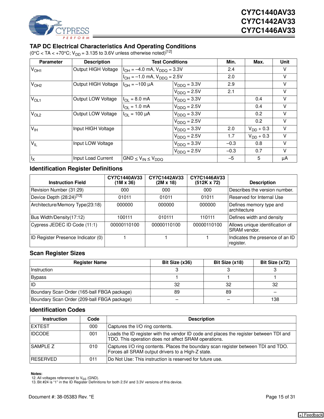
TAP DC Electrical Characteristics And Operating Conditions
(0°C < TA < +70°C; V = 3.135 to 3.6V unless otherwise noted)[12] |
|
|
|
| ||
| DD |
|
|
|
|
|
Parameter | Description | Test Conditions | Min. | Max. | Unit | |
VOH1 | Output HIGH Voltage | IOH = | 2.4 |
| V | |
|
| IOH = | 2.0 |
| V | |
VOH2 | Output HIGH Voltage | IOH = | VDDQ = 3.3V | 2.9 |
| V |
|
|
| VDDQ = 2.5V | 2.1 |
| V |
VOL1 | Output LOW Voltage | IOL = 8.0 mA | VDDQ = 3.3V |
| 0.4 | V |
|
| IOL = 1.0 mA | VDDQ = 2.5V |
| 0.4 | V |
VOL2 | Output LOW Voltage | IOL = 100 µA | VDDQ = 3.3V |
| 0.2 | V |
|
|
| VDDQ = 2.5V |
| 0.2 | V |
VIH | Input HIGH Voltage |
| VDDQ = 3.3V | 2.0 | VDD + 0.3 | V |
|
|
| VDDQ = 2.5V | 1.7 | VDD + 0.3 | V |
VIL | Input LOW Voltage |
| VDDQ = 3.3V | 0.8 | V | |
|
|
| VDDQ = 2.5V | 0.7 | V | |
IX | Input Load Current | GND < VIN < VDDQ |
| 5 | µA | |
Identification Register Definitions
Instruction Field | CY7C1440AV33 | CY7C1442AV33 | CY7C1446AV33 | Description |
(1M x 36) | (2M x 18) | (512K x 72) | ||
|
|
|
|
|
Revision Number (31:29) | 000 | 000 | 000 | Describes the version number. |
|
|
|
|
|
Device Depth (28:24)[13] | 01011 | 01011 | 01011 | Reserved for Internal Use |
Architecture/Memory Type(23:18) | 000000 | 000000 | 000000 | Defines memory type and |
|
|
|
| architecture |
Bus Width/Density(17:12) | 100111 | 010111 | 110111 | Defines width and density |
|
|
|
|
|
Cypress JEDEC ID Code (11:1) | 00000110100 | 00000110100 | 00000110100 | Allows unique identification of |
|
|
|
| SRAM vendor. |
ID Register Presence Indicator (0) | 1 | 1 | 1 | Indicates the presence of an ID |
|
|
|
| register. |
Scan Register Sizes
Register Name | Bit Size (x36) | Bit Size (x18) | Bit Size (x72) |
Instruction | 3 | 3 | 3 |
|
|
|
|
Bypass | 1 | 1 | 1 |
|
|
|
|
ID | 32 | 32 | 32 |
|
|
|
|
Boundary Scan Order | 89 | 89 | – |
|
|
|
|
Boundary Scan Order | – | – | 138 |
|
|
|
|
Identification Codes
Instruction | Code | Description |
EXTEST | 000 | Captures the I/O ring contents. |
|
|
|
IDCODE | 001 | Loads the ID register with the vendor ID code and places the register between TDI and |
|
| TDO. This operation does not affect SRAM operations. |
SAMPLE Z | 010 | Captures I/O ring contents. Places the boundary scan register between TDI and TDO. |
|
| Forces all SRAM output drivers to a |
RESERVED | 011 | Do Not Use: This instruction is reserved for future use. |
|
|
|
Notes:
12.All voltages referenced to VSS (GND).
13.Bit #24 is “1” in the ID Register Definitions for both 2.5V and 3.3V versions of this device.
Document #: | Page 15 of 31 |
[+] Feedback