CY7C1440AV33
CY7C1442AV33
CY7C1446AV33
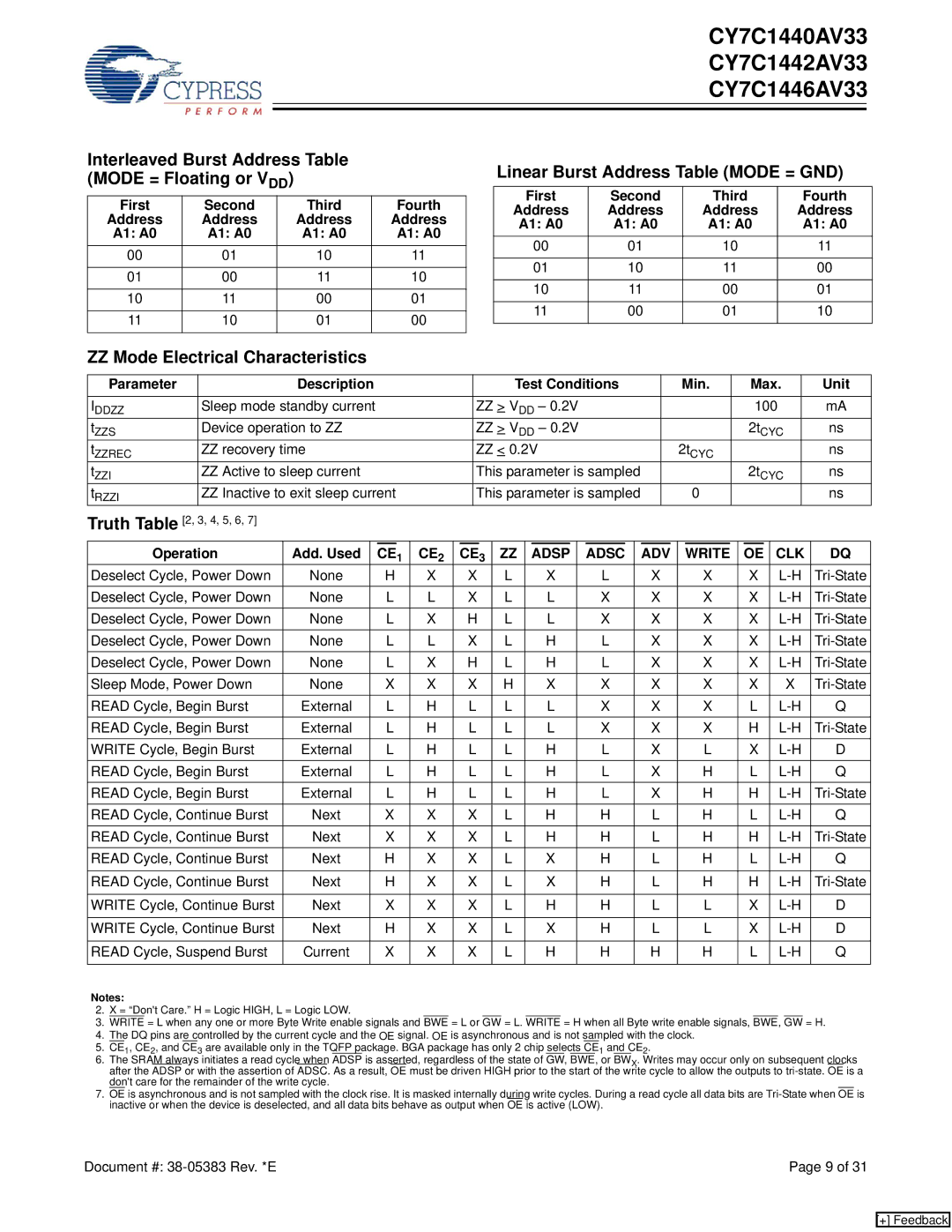
Interleaved Burst Address Table (MODE = Floating or VDD)
First | Second | Third | Fourth |
Address | Address | Address | Address |
A1: A0 | A1: A0 | A1: A0 | A1: A0 |
00 | 01 | 10 | 11 |
|
|
|
|
01 | 00 | 11 | 10 |
|
|
|
|
10 | 11 | 00 | 01 |
|
|
|
|
11 | 10 | 01 | 00 |
|
|
|
|
Linear Burst Address Table (MODE = GND)
First | Second | Third | Fourth |
Address | Address | Address | Address |
A1: A0 | A1: A0 | A1: A0 | A1: A0 |
00 | 01 | 10 | 11 |
|
|
|
|
01 | 10 | 11 | 00 |
|
|
|
|
10 | 11 | 00 | 01 |
|
|
|
|
11 | 00 | 01 | 10 |
|
|
|
|
ZZ Mode Electrical Characteristics
Parameter |
| Description |
|
|
|
|
|
|
| Test Conditions |
|
|
| Min. |
|
| Max. |
| Unit | |||||||||||||
IDDZZ |
| Sleep mode standby current |
|
|
|
|
| ZZ > VDD – 0.2V |
|
|
|
|
|
|
|
|
|
|
| 100 |
| mA | ||||||||||
tZZS |
| Device operation to ZZ |
|
|
|
|
| ZZ > VDD – 0.2V |
|
|
|
|
|
|
|
|
|
|
| 2tCYC |
| ns | ||||||||||
tZZREC |
| ZZ recovery time |
|
|
|
|
| ZZ < 0.2V |
|
|
|
|
|
| 2tCYC |
|
|
|
|
|
| ns | ||||||||||
tZZI |
| ZZ Active to sleep current |
|
|
|
|
| This parameter is sampled |
|
|
|
|
|
|
|
| 2tCYC |
| ns | |||||||||||||
tRZZI |
| ZZ Inactive to exit sleep current |
|
|
| This parameter is sampled |
|
| 0 |
|
|
|
|
|
|
| ns | |||||||||||||||
Truth Table [2, 3, 4, 5, 6, 7] |
|
|
|
|
|
|
|
|
|
|
|
|
|
|
|
|
|
|
|
|
|
|
|
|
|
|
|
|
|
| ||
| Operation | Add. Used |
| CE | 1 | CE2 |
| CE | 3 | ZZ |
| ADSP |
|
| ADSC |
|
| ADV |
|
| WRITE |
|
|
| OE |
| CLK | DQ | ||||
Deselect Cycle, Power Down | None |
| H | X |
| X | L |
| X |
| L |
| X |
|
| X |
| X |
| |||||||||||||
Deselect Cycle, Power Down | None |
| L | L |
| X | L |
| L |
| X |
| X |
|
| X |
| X |
| |||||||||||||
Deselect Cycle, Power Down | None |
| L | X |
| H | L |
| L |
| X |
| X |
|
| X |
| X |
| |||||||||||||
Deselect Cycle, Power Down | None |
| L | L |
| X | L |
| H |
| L |
| X |
|
| X |
| X |
| |||||||||||||
Deselect Cycle, Power Down | None |
| L | X |
| H | L |
| H |
| L |
| X |
|
| X |
| X |
| |||||||||||||
Sleep Mode, Power Down | None |
| X | X |
| X | H |
| X |
| X |
| X |
|
| X |
| X |
| X | ||||||||||||
READ Cycle, Begin Burst | External |
| L | H |
| L | L |
| L |
| X |
| X |
|
| X |
| L |
| Q | ||||||||||||
READ Cycle, Begin Burst | External |
| L | H |
| L | L |
| L |
| X |
| X |
|
| X |
| H |
| |||||||||||||
WRITE Cycle, Begin Burst | External |
| L | H |
| L | L |
| H |
| L |
| X |
|
| L |
| X |
| D | ||||||||||||
READ Cycle, Begin Burst | External |
| L | H |
| L | L |
| H |
| L |
| X |
|
| H |
| L |
| Q | ||||||||||||
READ Cycle, Begin Burst | External |
| L | H |
| L | L |
| H |
| L |
| X |
|
| H |
| H |
| |||||||||||||
READ Cycle, Continue Burst | Next |
| X | X |
| X | L |
| H |
| H |
| L |
|
| H |
| L |
| Q | ||||||||||||
READ Cycle, Continue Burst | Next |
| X | X |
| X | L |
| H |
| H |
| L |
|
| H |
| H |
| |||||||||||||
READ Cycle, Continue Burst | Next |
| H | X |
| X | L |
| X |
| H |
| L |
|
| H |
| L |
| Q | ||||||||||||
|
|
|
|
|
|
|
|
|
|
|
|
|
|
|
|
|
|
|
|
|
| |||||||||||
READ Cycle, Continue Burst | Next |
| H | X |
| X | L |
| X |
| H |
| L |
|
| H |
| H |
| |||||||||||||
|
|
|
|
|
|
|
|
|
|
|
|
|
|
|
|
|
|
|
|
|
| |||||||||||
WRITE Cycle, Continue Burst | Next |
| X | X |
| X | L |
| H |
| H |
| L |
|
| L |
| X |
| D | ||||||||||||
|
|
|
|
|
|
|
|
|
|
|
|
|
|
|
|
|
|
|
|
|
| |||||||||||
WRITE Cycle, Continue Burst | Next |
| H | X |
| X | L |
| X |
| H |
| L |
|
| L |
| X |
| D | ||||||||||||
|
|
|
|
|
|
|
|
|
|
|
|
|
|
|
|
|
|
|
|
|
| |||||||||||
READ Cycle, Suspend Burst | Current |
| X | X |
| X | L |
| H |
| H |
| H |
|
| H |
| L |
| Q | ||||||||||||
|
|
|
|
|
|
|
|
|
|
|
|
|
|
|
|
|
|
|
|
|
|
|
|
|
|
|
|
|
|
|
|
|
Notes:
2.X = “Don't Care.” H = Logic HIGH, L = Logic LOW.
3.WRITE = L when any one or more Byte Write enable signals and BWE = L or GW = L. WRITE = H when all Byte write enable signals, BWE, GW = H.
4.The DQ pins are controlled by the current cycle and the OE signal. OE is asynchronous and is not sampled with the clock.
5.CE1, CE2, and CE3 are available only in the TQFP package. BGA package has only 2 chip selects CE1 and CE2.
6.The SRAM always initiates a read cycle when ADSP is asserted, regardless of the state of GW, BWE, or BWX. Writes may occur only on subsequent clocks after the ADSP or with the assertion of ADSC. As a result, OE must be driven HIGH prior to the start of the write cycle to allow the outputs to
7.OE is asynchronous and is not sampled with the clock rise. It is masked internally during write cycles. During a read cycle all data bits are
Document #: | Page 9 of 31 |
[+] Feedback