CY7C1440AV33
CY7C1442AV33
CY7C1446AV33
Document History Page
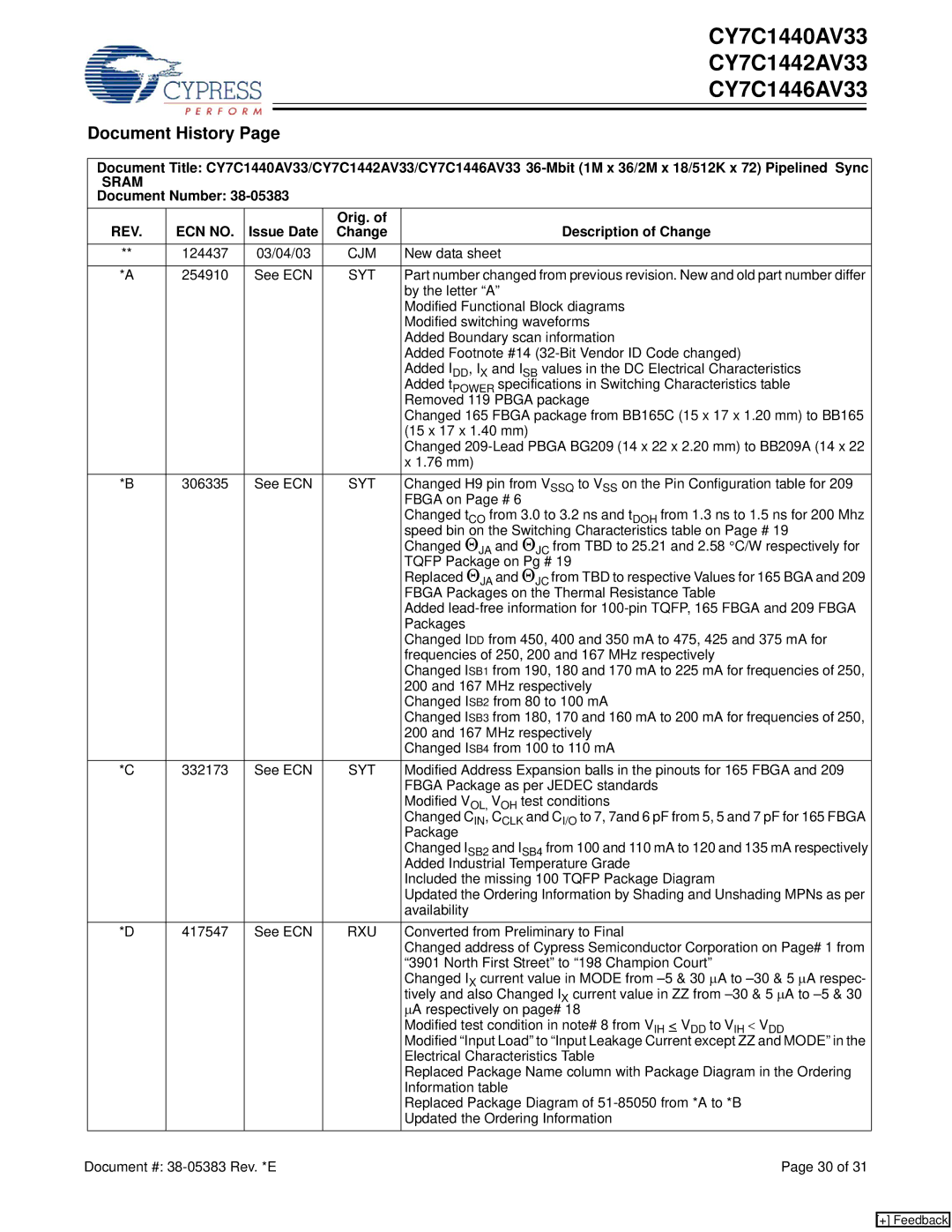
| Document Title: CY7C1440AV33/CY7C1442AV33/CY7C1446AV33 | ||||
| SRAM |
|
|
|
|
| Document Number: |
|
| ||
| REV. | ECN NO. | Issue Date | Orig. of | Description of Change |
| Change | ||||
| ** | 124437 | 03/04/03 | CJM | New data sheet |
|
|
|
|
|
|
| *A | 254910 | See ECN | SYT | Part number changed from previous revision. New and old part number differ |
|
|
|
|
| by the letter “A” |
|
|
|
|
| Modified Functional Block diagrams |
|
|
|
|
| Modified switching waveforms |
|
|
|
|
| Added Boundary scan information |
|
|
|
|
| Added Footnote #14 |
|
|
|
|
| Added IDD, IX and ISB values in the DC Electrical Characteristics |
|
|
|
|
| Added tPOWER specifications in Switching Characteristics table |
|
|
|
|
| Removed 119 PBGA package |
|
|
|
|
| Changed 165 FBGA package from BB165C (15 x 17 x 1.20 mm) to BB165 |
|
|
|
|
| (15 x 17 x 1.40 mm) |
|
|
|
|
| Changed |
|
|
|
|
| x 1.76 mm) |
| *B | 306335 | See ECN | SYT | Changed H9 pin from VSSQ to VSS on the Pin Configuration table for 209 |
|
|
|
|
| FBGA on Page # 6 |
|
|
|
|
| Changed tCO from 3.0 to 3.2 ns and tDOH from 1.3 ns to 1.5 ns for 200 Mhz |
|
|
|
|
| speed bin on the Switching Characteristics table on Page # 19 |
|
|
|
|
| Changed ΘJA and ΘJC from TBD to 25.21 and 2.58 °C/W respectively for |
|
|
|
|
| TQFP Package on Pg # 19 |
|
|
|
|
| Replaced ΘJA and ΘJC from TBD to respective Values for 165 BGA and 209 |
|
|
|
|
| FBGA Packages on the Thermal Resistance Table |
|
|
|
|
| Added |
|
|
|
|
| Packages |
|
|
|
|
| Changed IDD from 450, 400 and 350 mA to 475, 425 and 375 mA for |
|
|
|
|
| frequencies of 250, 200 and 167 MHz respectively |
|
|
|
|
| Changed ISB1 from 190, 180 and 170 mA to 225 mA for frequencies of 250, |
|
|
|
|
| 200 and 167 MHz respectively |
|
|
|
|
| Changed ISB2 from 80 to 100 mA |
|
|
|
|
| Changed ISB3 from 180, 170 and 160 mA to 200 mA for frequencies of 250, |
|
|
|
|
| 200 and 167 MHz respectively |
|
|
|
|
| Changed ISB4 from 100 to 110 mA |
| *C | 332173 | See ECN | SYT | Modified Address Expansion balls in the pinouts for 165 FBGA and 209 |
|
|
|
|
| FBGA Package as per JEDEC standards |
|
|
|
|
| Modified VOL, VOH test conditions |
|
|
|
|
| Changed CIN, CCLK and CI/O to 7, 7and 6 pF from 5, 5 and 7 pF for 165 FBGA |
|
|
|
|
| Package |
|
|
|
|
| Changed ISB2 and ISB4 from 100 and 110 mA to 120 and 135 mA respectively |
|
|
|
|
| Added Industrial Temperature Grade |
|
|
|
|
| Included the missing 100 TQFP Package Diagram |
|
|
|
|
| Updated the Ordering Information by Shading and Unshading MPNs as per |
|
|
|
|
| availability |
| *D | 417547 | See ECN | RXU | Converted from Preliminary to Final |
|
|
|
|
| Changed address of Cypress Semiconductor Corporation on Page# 1 from |
|
|
|
|
| “3901 North First Street” to “198 Champion Court” |
|
|
|
|
| Changed IX current value in MODE from |
|
|
|
|
| tively and also Changed IX current value in ZZ from |
|
|
|
|
| ∝A respectively on page# 18 |
|
|
|
|
| Modified test condition in note# 8 from VIH < VDD to VIH < VDD |
|
|
|
|
| Modified “Input Load” to “Input Leakage Current except ZZ and MODE” in the |
|
|
|
|
| Electrical Characteristics Table |
|
|
|
|
| Replaced Package Name column with Package Diagram in the Ordering |
|
|
|
|
| Information table |
|
|
|
|
| Replaced Package Diagram of |
|
|
|
|
| Updated the Ordering Information |
Document #: |
| Page 30 of 31 | |||
[+] Feedback
