CY7C1440AV33
CY7C1442AV33
CY7C1446AV33
Switching Waveforms (continued)
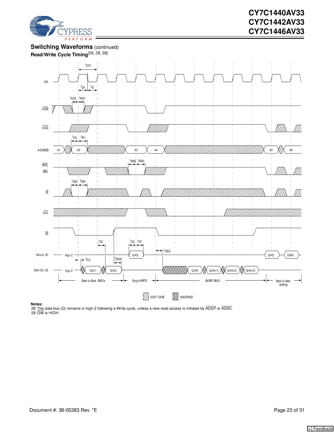
Read/Write Cycle Timing[26, 28, 29]
|
|
| tCYC |
CLK |
|
|
|
|
| tCH | tCL |
| tADS | tADH |
|
ADSP |
|
|
|
ADSC |
|
|
|
| tAS | tAH |
|
ADDRESS | A1 | A2 |
|
BWE, |
|
|
|
BWX |
|
|
|
| tCES | tCEH |
|
CE |
|
|
|
ADV |
|
|
|
OE |
|
|
|
|
|
| tCO |
A3 A4
tWES tWEH
tDS tDH
A5 A6
Data In (D) | t | tOEHZ | |
|
| ||
|
| CLZ |
|
Data Out (Q) | Q(A1) | Q(A2) |
D(A3)
![]()
![]()
![]() tOELZ
tOELZ
Q(A4) ![]() Q(A4+1)
Q(A4+1) ![]() Q(A4+2)
Q(A4+2) ![]() Q(A4+3)
Q(A4+3)
D(A5) D(A6)
Single WRITE | BURST READ |
DON’T CARE | UNDEFINED |
WRITEs
Notes:
28.The data bus (Q) remains in
29.GW is HIGH.
Document #: | Page 23 of 31 |
[+] Feedback