
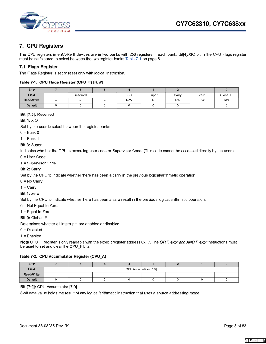
CY7C638xx, CY7C63310 specifications
The Cypress CY7C63310 and CY7C638xx series are advanced USB microcontrollers designed for various applications requiring reliable performance and flexibility. These chips are notable for their integration of several key technologies, enabling developers to create innovative electronic designs effortlessly.The CY7C63310 is a part of the Cypress USB microcontroller family that boasts a fully integrated 8051-compatible microprocessor core. This architecture allows for efficient execution of high-level programming languages like C, enhancing code development efforts. The microcontroller supports USB 2.0 full-speed operation, allowing for high data transfer rates of up to 12 Mbps, essential for applications involving data communication.
One of the standout features of the CY7C63310 is its programmable GPIO (General-Purpose Input/Output) pins, which provide developers with the versatility to configure these pins as inputs, outputs, or alternate functions. This flexibility is particularly advantageous in applications where custom interfaces are essential, such as human-machine interfaces, sensor control, and USB peripherals.
Moreover, the CY7C638xx series presents an even broader array of features. These devices typically support various memory configurations, enabling designers to select from different on-chip RAM and flash memory options. This variety empowers projects requiring a mix of program and data storage capabilities, all while ensuring that performance remains optimal.
Both the CY7C63310 and CY7C638xx series leverage Cypress's EZ-USB technology, which simplifies the process of USB interface implementation. The EZ-USB architecture minimizes the effort associated with USB protocol complexity, allowing developers to focus on the core functionality of their applications.
These microcontrollers also incorporate features such as low-power operation, making them ideal for battery-operated devices. With various power management modes, designers can optimize energy consumption according to the specific needs of their applications.
In terms of connectivity, these chips support multiple interface standards, including SPI, I2C, and UART. These capabilities ensure that developers can easily interface with other components and systems, enhancing the overall utility of the microcontroller.
In summary, the Cypress CY7C63310 and CY7C638xx microcontrollers stand out for their robust features, including integrated USB functionality, flexible GPIO options, and support for various communication protocols. These attributes make them suitable for a wide range of applications, from consumer electronics to industrial automation, making them an excellent choice for developers seeking reliable and adaptable microcontroller solutions.