CYDC256B16, CYDC128B16,
CYDC064B16, CYDC128B08,
CYDC064B08
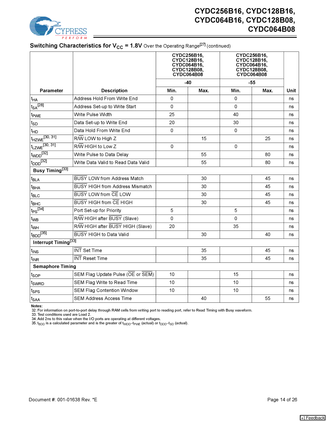
Switching Characteristics for V = 1.8V Over the Operating Range[27] (continued) |
|
|
|
| |||||||||||||||||||||||
|
|
|
|
|
|
|
|
|
|
|
| CC |
|
|
|
|
|
|
|
| |||||||
|
|
|
|
|
|
|
|
|
|
|
|
|
|
|
|
|
|
|
| CYDC256B16, |
| CYDC256B16, |
| ||||
|
|
|
|
|
|
|
|
|
|
|
|
|
|
|
|
|
|
|
| CYDC128B16, |
| CYDC128B16, |
| ||||
|
|
|
|
|
|
|
|
|
|
|
|
|
|
|
|
|
|
|
| CYDC064B16, |
| CYDC064B16, |
| ||||
|
|
|
|
|
|
|
|
|
|
|
|
|
|
|
|
|
|
|
| CYDC128B08, |
| CYDC128B08, |
| ||||
|
|
|
|
|
|
|
|
|
|
|
|
|
|
|
|
|
|
|
| CYDC064B08 |
| CYDC064B08 |
| ||||
|
|
|
|
|
|
|
|
|
|
|
|
|
|
|
|
|
|
|
|
|
|
|
| ||||
Parameter |
|
|
|
|
|
|
|
| Description |
|
|
|
|
|
|
| Unit | ||||||||||
|
|
|
|
|
|
|
| Min. |
| Max. |
| Min. |
| Max. | |||||||||||||
|
|
|
|
|
|
|
|
|
|
| |||||||||||||||||
tHA |
| Address Hold From Write End | 0 |
|
|
| 0 |
|
| ns | |||||||||||||||||
tSA[28] |
| Address | 0 |
|
|
| 0 |
|
| ns | |||||||||||||||||
tPWE |
| Write Pulse Width | 25 |
|
|
| 40 |
|
| ns | |||||||||||||||||
tSD |
| Data | 20 |
|
|
| 30 |
|
| ns | |||||||||||||||||
tHD |
| Data Hold From Write End | 0 |
|
|
| 0 |
|
| ns | |||||||||||||||||
tHZWE[30, 31] |
|
|
|
|
|
|
|
|
|
|
|
|
|
|
|
|
|
|
|
|
|
|
|
|
|
|
|
R/W | LOW to High Z |
|
| 15 |
|
|
| 25 | ns | ||||||||||||||||||
tLZWE[30, 31] |
|
|
|
|
|
|
|
|
|
|
|
|
|
|
|
|
|
|
|
|
|
|
|
|
|
|
|
R/W | HIGH to Low Z | 0 |
|
|
| 0 |
|
| ns | ||||||||||||||||||
tWDD[32] |
| Write Pulse to Data Delay |
|
| 55 |
|
|
| 80 | ns | |||||||||||||||||
tDDD[32] |
| Write Data Valid to Read Data Valid |
|
| 55 |
|
|
| 80 | ns | |||||||||||||||||
Busy Timing[33] |
|
|
|
|
|
|
|
|
|
|
|
|
|
|
|
|
|
|
|
|
|
|
|
|
|
|
|
tBLA |
| BUSY |
| LOW from Address Match |
|
| 30 |
|
|
| 45 | ns | |||||||||||||||
tBHA |
|
|
|
|
|
|
|
| HIGH from Address Mismatch |
|
| 30 |
|
|
| 45 | ns | ||||||||||
BUSY |
|
| |||||||||||||||||||||||||
tBLC |
|
|
|
|
|
|
|
| LOW from |
|
|
| LOW |
|
| 30 |
|
|
| 45 | ns | ||||||
BUSY | CE |
|
| ||||||||||||||||||||||||
tBHC |
|
|
|
|
|
|
|
| HIGH from |
|
| HIGH |
|
| 30 |
|
|
| 45 | ns | |||||||
BUSY | CE |
|
| ||||||||||||||||||||||||
tPS[34] |
| Port | 5 |
|
|
| 5 |
|
| ns | |||||||||||||||||
tWB |
|
|
|
|
|
|
|
|
|
|
|
|
|
|
|
|
|
|
|
|
|
|
|
|
|
|
|
R/W | HIGH after BUSY (Slave) | 0 |
|
|
| 0 |
|
| ns | ||||||||||||||||||
tWH |
|
|
|
|
|
| HIGH after |
|
|
|
|
| HIGH (Slave) | 20 |
|
|
| 35 |
|
| ns | ||||||
R/W | BUSY |
|
|
|
|
| |||||||||||||||||||||
tBDD[35] |
|
|
|
|
|
|
| HIGH to Data Valid |
|
| 30 |
|
|
| 40 | ns | |||||||||||
BUSY |
|
| |||||||||||||||||||||||||
Interrupt Timing[33] |
|
|
|
|
|
|
|
| |||||||||||||||||||
tINS |
| INT |
| Set Time |
|
| 35 |
|
|
| 45 | ns | |||||||||||||||
tINR |
|
|
|
| Reset Time |
|
| 35 |
|
|
| 45 | ns | ||||||||||||||
INT |
|
| |||||||||||||||||||||||||
Semaphore Timing |
|
|
|
|
|
|
|
| |||||||||||||||||||
|
|
|
|
|
|
|
|
|
|
|
|
|
| ||||||||||||||
tSOP |
| SEM Flag Update Pulse | (OE | or | SEM) |
| 10 |
|
|
| 15 |
|
| ns | |||||||||||||
tSWRD |
| SEM Flag Write to Read Time | 10 |
|
|
| 10 |
|
| ns | |||||||||||||||||
tSPS |
| SEM Flag Contention Window | 10 |
|
|
| 10 |
|
| ns | |||||||||||||||||
tSAA |
| SEM Address Access Time |
|
| 40 |
|
|
| 55 | ns | |||||||||||||||||
Notes:
32.For information on
33.Test conditions used are Load 2.
34.Add 2ns to this value when the I/O ports are operating at different voltages.
35.tBDD is a calculated parameter and is the greater of
Document #: | Page 14 of 26 |
[+] Feedback