CYDC256B16, CYDC128B16,
CYDC064B16, CYDC128B08,
CYDC064B08
Switching Waveforms (continued)
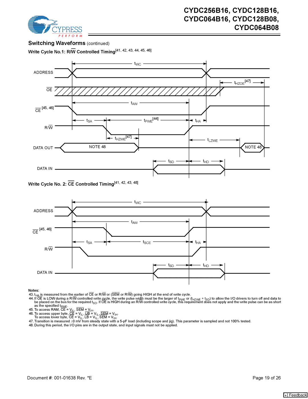
Write Cycle No.1: R/W Controlled Timing[41, 42, 43, 44, 45, 46] |
| ||
|
| tWC |
|
ADDRESS |
|
|
|
|
|
| tHZOE[47] |
OE |
|
|
|
CE [45, 46] |
| tAW |
|
|
|
| |
| tSA | tPWE[44] | tHA |
R/W |
|
|
|
|
| tHZWE[47] | tLZWE |
DATA OUT | NOTE 48 |
| NOTE 48 |
|
| tSD | tHD |
DATA IN |
|
|
|
Write Cycle No. 2: CE Controlled Timing[41, 42, 43, 48] |
|
|
tWC |
|
|
ADDRESS |
|
|
tAW |
|
|
CE [45, 46] |
|
|
tSA | tSCE | tHA |
R/W |
|
|
| tSD | tHD |
DATA IN |
|
|
Notes:
43.tHA is measured from the earlier of CE or R/W or (SEM or R/W) going HIGH at the end of write cycle.
44.If OE is LOW during a R/W controlled write cycle, the write pulse width must be the larger of tPWE or (tHZWE + tSD) to allow the I/O drivers to turn off and data to be placed on the bus for the required tSD. If OE is HIGH during an R/W controlled write cycle, this requirement does not apply and the write pulse can be as short as the specified tPWE.
45.To access RAM, CE = VIL, SEM = VIH.
46.To access upper byte, CE = VIL, UB = VIL, SEM = VIH. To access lower byte, CE = VIL, LB = VIL, SEM = VIH.
47.Transition is measured ±0 mV from steady state with a
48.During this period, the I/O pins are in the output state, and input signals must not be applied.
Document #: | Page 19 of 26 |
[+] Feedback