CYDC256B16, CYDC128B16,
CYDC064B16, CYDC128B08,
CYDC064B08
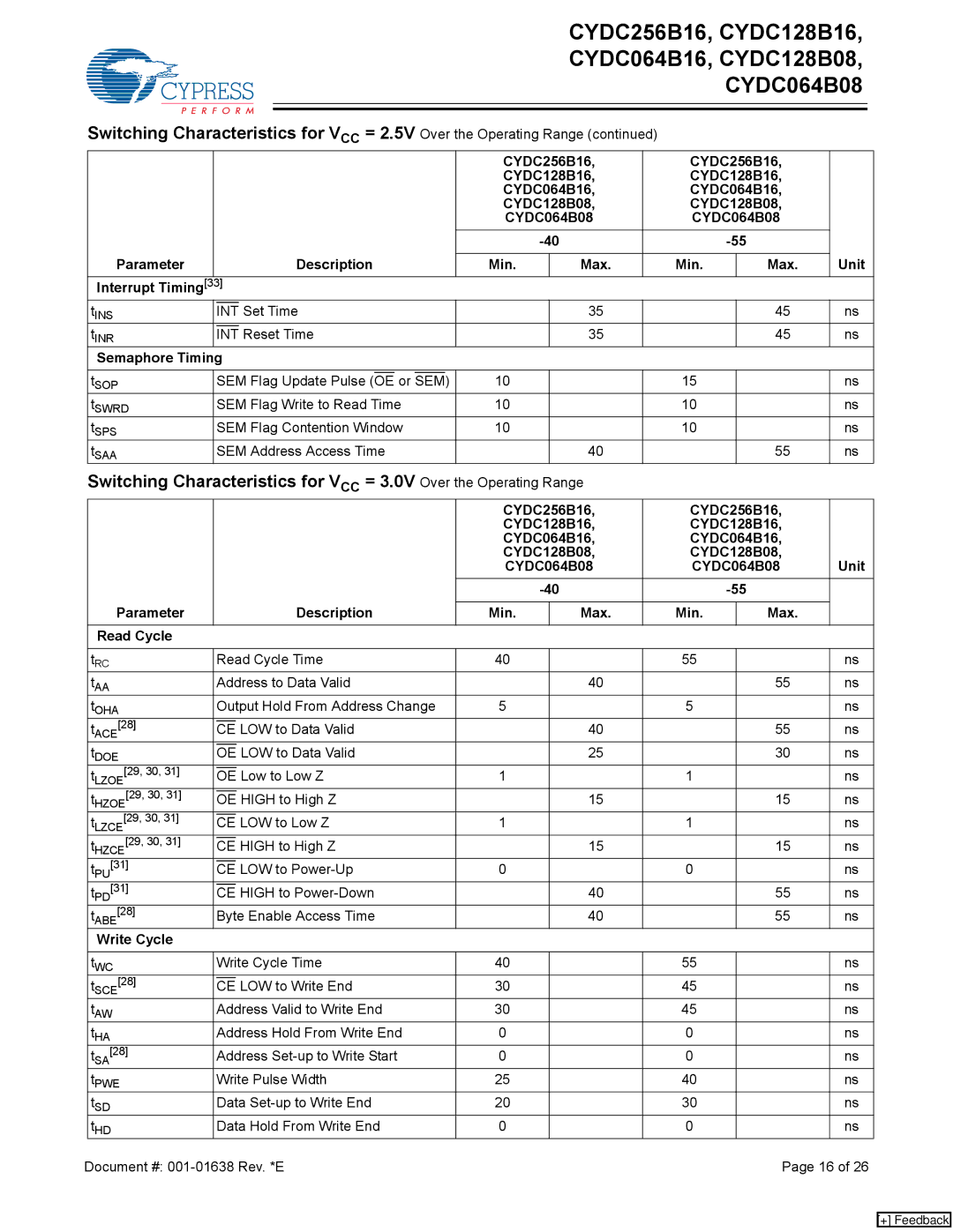
Switching Characteristics for VCC = 2.5V Over the Operating Range (continued)
|
|
|
|
|
|
|
|
| CYDC256B16, | CYDC256B16, |
| ||||
|
|
|
|
|
|
|
|
| CYDC128B16, | CYDC128B16, |
| ||||
|
|
|
|
|
|
|
|
| CYDC064B16, | CYDC064B16, |
| ||||
|
|
|
|
|
|
|
|
| CYDC128B08, | CYDC128B08, |
| ||||
|
|
|
|
|
|
|
|
| CYDC064B08 | CYDC064B08 |
| ||||
|
|
|
|
|
|
|
|
|
|
|
| ||||
Parameter |
|
|
| Description |
|
|
|
|
|
| Unit | ||||
|
|
| Min. |
| Max. | Min. |
| Max. | |||||||
|
|
|
|
|
|
|
|
| |||||||
Interrupt Timing[33] |
|
|
|
|
|
|
| ||||||||
tINS |
| INT |
| Set Time |
|
| 35 |
|
| 45 | ns | ||||
tINR |
|
|
| Reset Time |
|
| 35 |
|
| 45 | ns | ||||
INT |
|
| |||||||||||||
Semaphore Timing |
|
|
|
|
|
|
| ||||||||
|
|
|
|
|
|
|
|
|
|
|
|
| |||
tSOP |
| SEM Flag Update Pulse | (OE | or | SEM) |
| 10 |
|
| 15 |
|
| ns | ||
tSWRD |
| SEM Flag Write to Read Time | 10 |
|
| 10 |
|
| ns | ||||||
tSPS |
| SEM Flag Contention Window | 10 |
|
| 10 |
|
| ns | ||||||
tSAA |
| SEM Address Access Time |
|
| 40 |
|
| 55 | ns | ||||||
Switching Characteristics for VCC = 3.0V Over the Operating Range
|
|
|
|
|
| CYDC256B16, | CYDC256B16, |
| ||||
|
|
|
|
|
| CYDC128B16, | CYDC128B16, |
| ||||
|
|
|
|
|
| CYDC064B16, | CYDC064B16, |
| ||||
|
|
|
|
|
| CYDC128B08, | CYDC128B08, | Unit | ||||
|
|
|
|
|
| CYDC064B08 | CYDC064B08 | |||||
|
|
|
|
|
|
|
|
| ||||
| Parameter |
|
|
| Description |
|
|
|
|
|
|
|
|
|
|
| Min. |
| Max. | Min. |
| Max. |
| ||
|
|
|
|
|
|
|
|
|
|
|
|
|
| Read Cycle |
|
|
|
|
|
|
|
|
|
| |
|
|
|
|
|
|
|
|
|
| |||
| tRC |
| Read Cycle Time | 40 |
|
| 55 |
|
| ns | ||
| tAA |
| Address to Data Valid |
|
| 40 |
|
| 55 | ns | ||
| tOHA |
| Output Hold From Address Change | 5 |
|
| 5 |
|
| ns | ||
| tACE[28] |
|
|
| LOW to Data Valid |
|
| 40 |
|
| 55 | ns |
CE |
|
| ||||||||||
| tDOE |
|
|
| LOW to Data Valid |
|
| 25 |
|
| 30 | ns |
OE |
|
| ||||||||||
| tLZOE[29, 30, 31] |
|
|
| Low to Low Z | 1 |
|
| 1 |
|
| ns |
OE |
|
|
|
| ||||||||
| tHZOE[29, 30, 31] |
|
|
| HIGH to High Z |
|
| 15 |
|
| 15 | ns |
OE |
|
| ||||||||||
| tLZCE[29, 30, 31] |
|
| LOW to Low Z | 1 |
|
| 1 |
|
| ns | |
CE |
|
|
|
| ||||||||
| tHZCE[29, 30, 31] |
|
| HIGH to High Z |
|
| 15 |
|
| 15 | ns | |
CE |
|
| ||||||||||
| tPU[31] |
|
| LOW to | 0 |
|
| 0 |
|
| ns | |
CE |
|
|
|
| ||||||||
| tPD[31] |
|
| HIGH to |
|
| 40 |
|
| 55 | ns | |
CE |
|
| ||||||||||
| tABE[28] |
| Byte Enable Access Time |
|
| 40 |
|
| 55 | ns | ||
| Write Cycle |
|
|
|
|
|
|
|
|
|
| |
|
|
|
|
|
|
|
|
|
| |||
| tWC |
| Write Cycle Time | 40 |
|
| 55 |
|
| ns | ||
| tSCE[28] |
|
| LOW to Write End | 30 |
|
| 45 |
|
| ns | |
CE |
|
|
|
| ||||||||
| tAW |
| Address Valid to Write End | 30 |
|
| 45 |
|
| ns | ||
| tHA |
| Address Hold From Write End | 0 |
|
| 0 |
|
| ns | ||
| tSA[28] |
| Address | 0 |
|
| 0 |
|
| ns | ||
| tPWE |
| Write Pulse Width | 25 |
|
| 40 |
|
| ns | ||
| tSD |
| Data | 20 |
|
| 30 |
|
| ns | ||
| tHD |
| Data Hold From Write End | 0 |
|
| 0 |
|
| ns | ||
Document #: |
|
|
|
|
| Page 16 of 26 | ||||||
[+] Feedback