CYDC256B16, CYDC128B16,
CYDC064B16, CYDC128B08,
CYDC064B08
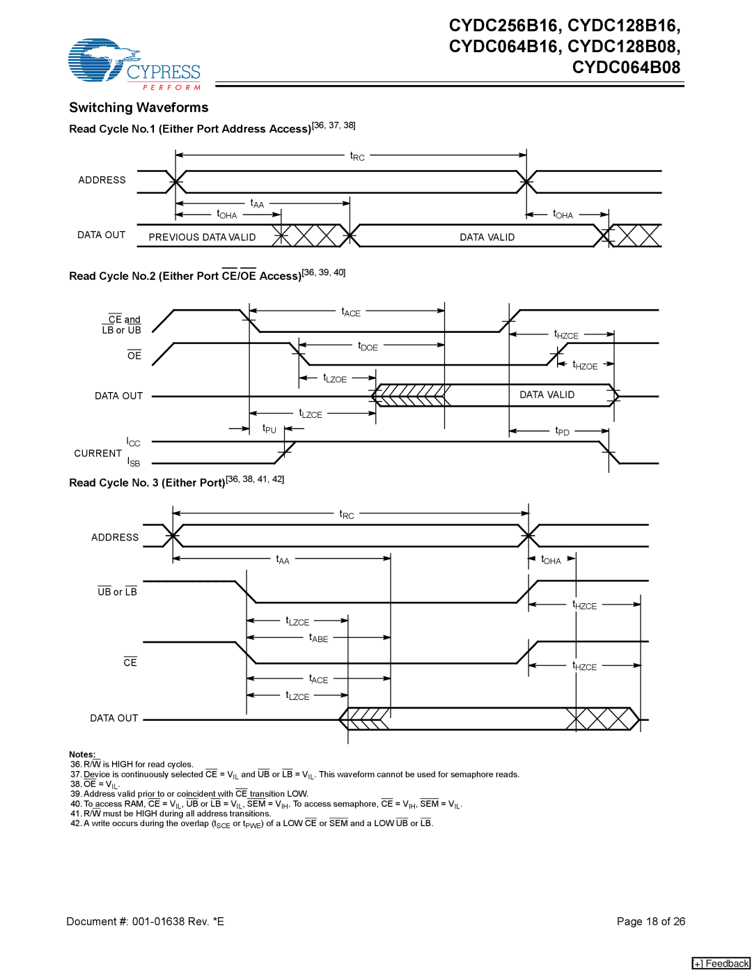
Switching Waveforms
Read Cycle No.1 (Either Port Address Access)[36, 37, 38]
|
| tRC |
ADDRESS |
|
|
| tAA | tOHA |
| tOHA | |
DATA OUT | PREVIOUS DATA VALID | DATA VALID |
Read Cycle No.2 (Either Port CE/OE Access)[36, 39, 40]
CE and
LB or UB
OE
DATA OUT
ICC
CURRENT
ISB
| tACE |
| tHZCE |
| tDOE |
| tHZOE |
| tLZOE |
| DATA VALID |
| tLZCE |
tPU | t |
| PD |
Read Cycle No. 3 (Either Port)[36, 38, 41, 42]
tRC
ADDRESS
tAA
UB or LB
tLZCE
tABE
CE
tACE
tLZCE
DATA OUT
tOHA
tHZCE |
tHZCE |
Notes:
36.R/W is HIGH for read cycles.
37.Device is continuously selected CE = VIL and UB or LB = VIL. This waveform cannot be used for semaphore reads.
38.OE = VIL.
39.Address valid prior to or coincident with CE transition LOW.
40.To access RAM, CE = VIL, UB or LB = VIL, SEM = VIH. To access semaphore, CE = VIH, SEM = VIL.
41.R/W must be HIGH during all address transitions.
42.A write occurs during the overlap (tSCE or tPWE) of a LOW CE or SEM and a LOW UB or LB.
Document #: | Page 18 of 26 |
[+] Feedback