CYDC256B16, CYDC128B16,
CYDC064B16, CYDC128B08,
CYDC064B08
Switching Waveforms (continued)
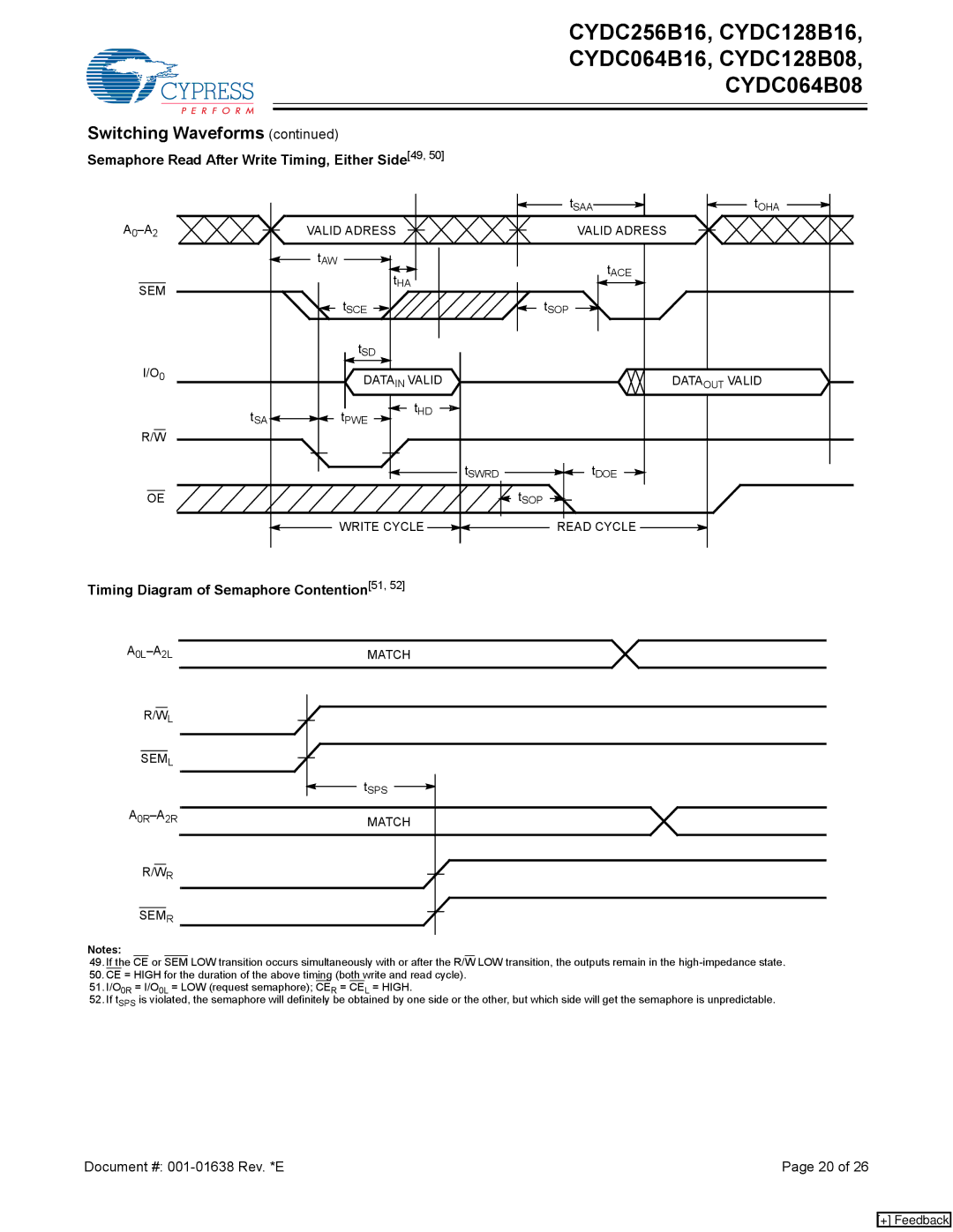
Semaphore Read After Write Timing, Either Side[49, 50]
|
| tSAA | tOHA |
VALID ADRESS | VALID ADRESS |
| |
| tAW | tACE |
|
| tHA |
| |
SEM |
|
| |
tSCE | tSOP |
| |
|
| ||
| tSD |
|
|
I/O0 | DATAIN VALID |
| DATAOUT VALID |
|
| ||
tSA | tHD |
|
|
tPWE |
|
| |
R/W |
|
|
|
| tSWRD | tDOE |
|
OE |
| tSOP |
|
| WRITE CYCLE | READ CYCLE |
|
Timing Diagram of Semaphore Contention[51, 52]
R/WL
SEML
R/WR
SEMR
MATCH
tSPS
MATCH
Notes:
49.If the CE or SEM LOW transition occurs simultaneously with or after the R/W LOW transition, the outputs remain in the
50.CE = HIGH for the duration of the above timing (both write and read cycle).
51.I/O0R = I/O0L = LOW (request semaphore); CER = CEL = HIGH.
52.If tSPS is violated, the semaphore will definitely be obtained by one side or the other, but which side will get the semaphore is unpredictable.
Document #: | Page 20 of 26 |
[+] Feedback