CYDC256B16, CYDC128B16, CYDC064B16, CYDC128B08, CYDC064B08
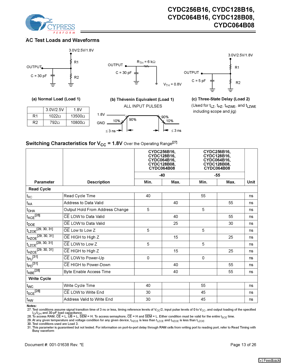
AC7Test Loads and Waveforms
|
|
|
|
|
|
|
|
| 3.0V/2.5V/1.8V |
|
|
|
|
|
|
|
|
|
| ||||||
OUTPUT |
|
|
|
|
|
|
|
|
|
|
|
|
| R1 | OUTPUT |
|
|
|
|
| RTH = 6 kΩ | ||||
|
|
|
|
|
|
|
|
|
|
|
|
| C = 30 pF |
|
|
|
|
|
|
| |||||
C = 30 pF |
|
|
|
|
|
|
|
|
|
|
|
| R2 |
|
|
|
|
|
|
| |||||
|
|
|
|
|
|
|
|
|
|
|
|
|
|
|
|
|
|
| |||||||
|
|
|
|
|
|
|
|
|
|
|
|
|
|
|
|
|
|
|
|
|
| ||||
|
|
|
|
|
|
|
|
|
|
|
|
|
|
|
|
|
|
|
|
|
|
|
|
|
|
|
|
|
|
|
|
|
|
|
|
|
|
|
|
|
|
|
|
|
|
|
|
|
|
|
|
|
|
|
|
|
|
|
|
|
|
|
|
|
|
|
|
|
|
|
|
|
|
|
|
|
|
OUTPUT ![]()
C = 5 pF
VTH = 0.8V
3.0V/2.5V/1.8V
R1
R2
(a) Normal Load (Load 1) |
|
| (b) Thévenin Equivalent (Load 1) | (c) | ||||||||||||||||
|
|
|
|
|
|
|
| ALL INPUT PULSES |
|
| (Used for tLZ, tHZ, tHZWE, and tLZWE | |||||||||
| 3.0V/2.5V | 1.8V | 1.8V |
|
|
|
|
|
|
|
|
|
|
|
|
|
|
|
| including scope and jig) |
|
|
|
|
|
|
|
|
|
|
|
|
|
|
|
|
|
|
| ||
R1 | 1022Ω | 13500Ω |
|
|
|
|
|
|
|
|
|
|
|
| 90% |
| ||||
|
|
|
| 10% |
|
|
|
|
|
| 90% |
|
|
|
| 10% |
| |||
R2 | 792Ω | 10800Ω | GND |
|
|
|
|
|
|
|
|
|
|
| ||||||
|
|
|
|
|
|
|
|
|
|
|
|
|
|
| ≤ 3 ns |
| ||||
|
|
|
| ≤ 3 ns |
|
|
|
|
|
|
|
|
|
|
|
|
| |||
|
|
|
|
|
|
|
|
|
|
|
|
|
|
|
|
| ||||
|
|
|
|
|
|
|
|
|
|
|
|
|
|
|
| |||||
Switching Characteristics for V = 1.8V Over the Operating Range[27] |
|
|
|
| |||||||
|
|
|
| CC |
|
|
|
|
|
|
|
|
|
|
|
| CYDC256B16, | CYDC256B16, |
| ||||
|
|
|
|
| CYDC128B16, | CYDC128B16, |
| ||||
|
|
|
|
| CYDC064B16, | CYDC064B16, |
| ||||
|
|
|
|
| CYDC128B08, | CYDC128B08, |
| ||||
|
|
|
|
| CYDC064B08 | CYDC064B08 |
| ||||
|
|
|
|
|
|
|
| ||||
Parameter |
|
|
| Description | Min. |
| Max. | Min. |
| Max. | Unit |
Read Cycle |
|
|
|
|
|
|
|
|
|
| |
tRC |
| Read Cycle Time | 40 |
|
| 55 |
|
| ns | ||
tAA |
| Address to Data Valid |
|
| 40 |
|
| 55 | ns | ||
tOHA |
| Output Hold From Address Change | 5 |
|
| 5 |
|
| ns | ||
tACE[28] |
|
|
| LOW to Data Valid |
|
| 40 |
|
| 55 | ns |
CE |
|
| |||||||||
tDOE |
|
|
| LOW to Data Valid |
|
| 25 |
|
| 30 | ns |
OE |
|
| |||||||||
tLZOE[29, 30, 31] |
|
|
| Low to Low Z | 5 |
|
| 5 |
|
| ns |
OE |
|
|
|
| |||||||
tHZOE[29, 30, 31] |
|
|
| HIGH to High Z |
|
| 15 |
|
| 25 | ns |
OE |
|
| |||||||||
tLZCE[29, 30, 31] |
|
| LOW to Low Z | 5 |
|
| 5 |
|
| ns | |
CE |
|
|
|
| |||||||
tHZCE[29, 30, 31] |
|
| HIGH to High Z |
|
| 15 |
|
| 25 | ns | |
CE |
|
| |||||||||
tPU[31] |
|
| LOW to | 0 |
|
| 0 |
|
| ns | |
CE |
|
|
|
| |||||||
tPD[31] |
|
| HIGH to |
|
| 40 |
|
| 55 | ns | |
CE |
|
| |||||||||
tABE[28] |
| Byte Enable Access Time |
|
| 40 |
|
| 55 | ns | ||
Write Cycle |
|
|
|
|
|
|
|
|
|
| |
|
|
|
|
|
|
|
|
| |||
tWC |
| Write Cycle Time | 40 |
|
| 55 |
|
| ns | ||
tSCE[28] |
|
| LOW to Write End | 30 |
|
| 45 |
|
| ns | |
CE |
|
|
|
| |||||||
tAW |
| Address Valid to Write End | 30 |
|
| 45 |
|
| ns | ||
Notes:
27.Test conditions assume signal transition time of 3 ns or less, timing reference levels of VCC/2, input pulse levels of 0 to VCC, and output loading of the specified IOI/IOH and
28.To access RAM, CE = L, UB = L, SEM = H. To access semaphore, CE = H and SEM = L. Either condition must be valid for the entire tSCE time.
29.At any given temperature and voltage condition for any given device, tHZCE is less than tLZCE and tHZOE is less than tLZOE.
30.Test conditions used are Load 3.
31.This parameter is guaranteed but not tested. For information on
Document #: | Page 13 of 26 |
[+] Feedback