CYDC256B16, CYDC128B16,
CYDC064B16, CYDC128B08,
CYDC064B08
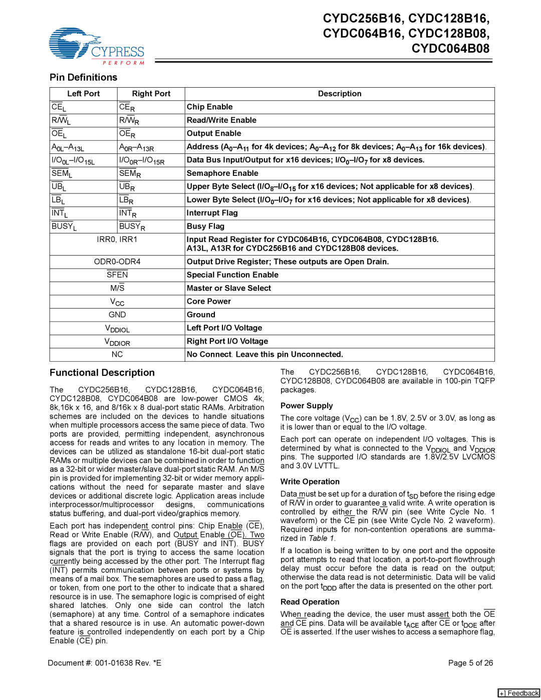
Pin Definitions
|
|
|
|
|
|
| Left Port |
|
|
|
|
|
|
|
|
|
| Right Port | Description | |||||
|
|
|
|
|
|
|
|
|
|
|
|
|
|
| ||||||||||
|
|
|
| L |
|
|
|
|
|
|
|
| R | Chip Enable | ||||||||||
| CE | CE | ||||||||||||||||||||||
|
|
|
|
|
|
| L |
|
|
|
|
|
|
|
|
|
|
| R | Read/Write Enable | ||||
| R/W |
|
|
| R/W | |||||||||||||||||||
|
|
|
|
| L |
|
|
|
|
|
|
|
|
| R | Output Enable | ||||||||
| OE |
|
|
| OE | |||||||||||||||||||
|
|
|
| Address | ||||||||||||||||||||
|
|
|
| Data Bus Input/Output for x16 devices; | ||||||||||||||||||||
|
|
|
|
|
|
|
| L |
|
|
|
|
|
|
|
|
|
|
|
| R | Semaphore Enable | ||
| SEM |
|
|
| SEM | |||||||||||||||||||
|
|
|
| L |
|
|
|
|
|
|
|
| R | Upper Byte Select | ||||||||||
| UB |
|
|
| UB | |||||||||||||||||||
|
|
| L |
|
|
|
|
|
|
| R | Lower Byte Select | ||||||||||||
| LB |
|
|
| LB | |||||||||||||||||||
|
|
|
|
|
| L |
|
|
|
|
|
|
|
|
|
| R | Interrupt Flag | ||||||
| INT |
|
|
| INT | |||||||||||||||||||
|
|
|
|
|
|
|
|
| L |
|
|
|
|
|
|
|
|
|
|
|
|
| R | Busy Flag |
| BUSY |
|
|
| BUSY | |||||||||||||||||||
|
|
|
|
|
|
|
|
| IRR0, IRR1 | Input Read Register for CYDC064B16, CYDC064B08, CYDC128B16. | ||||||||||||||
|
|
|
|
|
|
|
|
|
|
|
|
|
|
|
|
|
|
|
|
|
|
|
| A13L, A13R for CYDC256B16 and CYDC128B08 devices. |
|
|
|
|
|
|
|
|
| Output Drive Register; These outputs are Open Drain. | |||||||||||||||
|
|
|
|
|
|
|
|
|
|
|
|
|
|
|
| |||||||||
|
|
|
|
|
|
|
|
|
|
|
|
|
|
|
|
| Special Function Enable | |||||||
|
|
|
|
|
|
|
|
|
|
| SFEN | |||||||||||||
|
|
|
|
|
|
|
|
|
|
|
|
|
|
|
|
|
|
|
|
|
|
|
| Master or Slave Select |
|
|
|
|
|
|
|
|
|
|
| M/S |
| ||||||||||||
|
|
|
|
|
|
|
|
|
|
| VCC | Core Power | ||||||||||||
|
|
|
|
|
|
|
|
|
|
| GND | Ground | ||||||||||||
|
|
|
|
|
|
|
|
|
|
|
| |||||||||||||
|
|
|
|
|
|
|
|
|
| VDDIOL | Left Port I/O Voltage | |||||||||||||
|
|
|
|
|
|
|
|
|
| VDDIOR | Right Port I/O Voltage | |||||||||||||
|
|
|
|
|
|
|
|
|
|
| NC | No Connect. Leave this pin Unconnected. | ||||||||||||
|
|
|
|
|
|
|
|
|
|
|
|
|
|
|
|
|
|
|
|
|
|
|
|
|
Functional Description
The CYDC256B16, CYDC128B16, CYDC064B16, CYDC128B08, CYDC064B08 are
Each port has independent control pins: Chip Enable (CE), Read or Write Enable (R/W), and Output Enable (OE). Two flags are provided on each port (BUSY and INT). BUSY signals that the port is trying to access the same location currently being accessed by the other port. The Interrupt flag (INT) permits communication between ports or systems by means of a mail box. The semaphores are used to pass a flag, or token, from one port to the other to indicate that a shared resource is in use. The semaphore logic is comprised of eight shared latches. Only one side can control the latch (semaphore) at any time. Control of a semaphore indicates that a shared resource is in use. An automatic
The CYDC256B16, CYDC128B16, CYDC064B16, CYDC128B08, CYDC064B08 are available in
Power Supply
The core voltage (VCC) can be 1.8V, 2.5V or 3.0V, as long as it is lower than or equal to the I/O voltage.
Each port can operate on independent I/O voltages. This is determined by what is connected to the VDDIOL and VDDIOR pins. The supported I/O standards are 1.8V/2.5V LVCMOS and 3.0V LVTTL.
Write Operation
Data must be set up for a duration of tSD before the rising edge of R/W in order to guarantee a valid write. A write operation is controlled by either the R/W pin (see Write Cycle No. 1 waveform) or the CE pin (see Write Cycle No. 2 waveform). Required inputs for
If a location is being written to by one port and the opposite port attempts to read that location, a
Read Operation
When reading the device, the user must assert both the OE and CE pins. Data will be available tACE after CE or tDOE after OE is asserted. If the user wishes to access a semaphore flag,
Document #: | Page 5 of 26 |
[+] Feedback